Category Archives: Hardware Hacking

RC2017/4: Introducing Arudino6502

This weekend I polished up my Arduino Day project and published it to GitHub for Retrochallenge 2017/04.

Introducing Arduino6502

https://github.com/davecheney/arduino6502

The repository contains an Arduino sketch that can be loaded on Arduino Mega boards (Arduino Uno’s can be accommodated by lowering the RAMSIZE value).

The sketch includes ROM images for AppleSoft Lite and Krusader symbolic assembler.

To run AppleSoft BASIC, enter

\
E000R

And you will be dropped into the BASIC prompt

>

Remember that the Apple 1 was an upper case only machine, so you should enter all letters in upper case.

Krusader is available at $F000

\
F000R

What’s next?

The project currently targets the 8 bit Atmel chips due to the tight coupling between the Atmega 2560’s hardware serial port and the simulated 6821 PIA. The mapping is good enough that, as long as you insert a delay of 200ms or greater between newlines, you can paste HEX files into the Woz monitor and run the resulting program.

However, while the Apple 1 came with 4k or 8k of RAM, modern recreations like the Replica 1 assume at least 32k of RAM, making most of the software written for these nouveau Apple 1’s out of reach of this project.

To overcome this my next effort will be to port the project to run on Cortex-M platforms like the Teensy 3.x or Arduino Due to get access to more SRAM.

Simulating minicomputers on microcontrollers

This is a short blog post to reference the slides from my builderscon 2016 presentation.

I had a great time at buildercon, the talks were varied and engaging from a wide selection of Japanese makers. I’m grateful to the builderscon organisers for accepting my talk and inviting me to present at the inaugural builderscon conference in Tokyo, Japan.

Slides:

Further reading:

Transistor logic fundamentals

Long time readers of this blog will know that when I’m not shilling for the Go language, my hobbies include electronics and retro computing. For me, projects like James Newman’s Megaprocessor, a computer built entirely from discrete components, is about as good as it gets.

James has recently finished construction of the Megaprocessor and has started to document it on YouTube, you should totally check it out. But this post isn’t about the Megaprocessor.

When I subscribed to the Megaprocessor channel on YouTube I discovered James has produced another series of videos focused on the fundamentals of implementing digital logic with transistors. In the three videos embedded below, James lays out the foundations of digital logic.

The first video describes (in James’ wonderfully understated manner) the operation of the simplest digital logic circuit; a voltage controlled inverter built with one transistor1.

In the second video, James adds a second transistor in series with the first and demonstrates the implementation of the NAND (Not AND) function2.

In the third video, by reorganising the transistors in parallel, James shows the circuit now implements the logical NOR (Not OR) function.

… and that’s it. There are more videos in James’ Stepping Stones video series, but with these three operations, NOT (inversion), NAND, and NOR, any combination of digital logic of any size can be created, as the Megaprocessor shows3.

Why is this important?

The circuits described in this set of videos feature far fewer transistors than you would find in real processor, but they are not simplified. The circuits described in this video were used in mainframe computers in the 1960’s and formed the basis for the integrated microprocessors of the 1970’s.

In these three videos James describes the entire foundation for contemporary computation. No matter how many layers of operating systems, networks, and source code abstraction you build on top, the fundamentals of computation and digital logic remain as simple as these three videos.

Notes and further reading

If you’re interested in learning more, here are a few suggestions for your own research.

  1. If you have no background in electronics a simple analogy for the relationships between voltage, current, and resistance is water flowing through a pipe. In this analogy, voltage represents water pressure, pushing water through the pipe. Current is the water itself. The volume of water in the pipe is a property of both the diameter of the pipe, and any resistance which may cause segments of the pipe to be less than full. Resistance, the final property, is any constriction or obstruction of the pipe. The higher the resistance, the more the pipe is constricted, reducing the amount of water (current) flowing through it.
  2. James’ tutorials use discrete TTL logic. TTL stands for Transistor to Transistor Logic, introduced in the early 1960’s by Sylvania (yes, the lightbulb makers). Before TTL there were at least two other forms of digital logic, what were they, and why did they succumb to TTL?
  3. James’ tutorials, and the Megaprocessor itself, use NPN transistors. If the Megaprocessor was shrunk down to a single integrated circuit it would most likely be implemented using NMOS logic. NMOS was very popular in the 70’s and early 80’s but has since given way to CMOS logic. What are the differences between NMOS and CMOS and why would James have chosen NMOS to implement the Megaprocessor?

Building an atmega1284p prototype

This project was featured on Hackaday and the Atmel blog.

For the next step in my Apple 1 replica project I decided I wanted to replace the Arduino Mega board with a bare Atmega MPU with the goal of producing a two chip solution — just the Atmel and the 6502, no glue logic or external support chips.

I had been stockpiling parts for this phase of the project for a while now, so I sat down to lay out the board based on a small 5×7 cm perfboard.

Perfboard sketch

Perfboard sketch

The trickiest piece was fitting the crystal and load capacitors into the design without disrupting to many of the other traces. It worked out well so I decided to add ICSP and FTDI headers and tried my hand at laying out the board using Fritzing.

Fritzing layout

Fritzing layout

The picture above is one of several designs I tried in Fritzing. I designed another that uses a flood fill ground plane to eliminate all the vias. We’ll see how that one turns out in a few weeks.

Rant: Cadsoft Eagle might be the industry standard, at least amongst open source hardware hackers, but it truly embodies the “worse is better” philosophy. Maybe one day my Altium Circuitmaker invitation will arrive (hint hint).

The finished product

The finished product

While I’m waiting for my PCBs to be delivered I decided to build a simplified version. The FTDI and ISCP headers have been left off as they are readily accessible from the headers on the left hand side.

Demo time


It worked, first time.

Bootloaders

The atmega1284p’s I ordered were unprogrammed. Getting Optiboot installed on them is handled nicely by Manicbug’s Mighty1284 Arduino support package.  There are only two small issues of note.

  1. Due to cross talk between the XTAL1 and RX0 pins, serial communication may be unreliable. The solution to this is configure the clock source to use Full Swing mode (rather than the default low power mode). This is done by setting the relevant fuse settings in boards.txt like so
    mighty_opt.bootloader.low_fuses=0xf7
  2. Mighty1284 only supports Arduino 1.0.x, not the newer 1.5.x betas. This might be an issue if you are a fan of the improvements in Ardunio 1.5.x as it doesn’t look like Mighty1284 is being updated.

Next steps

I’m smitten with the 1284p. It feels like the right compromise between the pin starved 328 and the unfriendly 2540 series. The 1284p supports more SRAM than either of its counterparts and ships in a package large enough that you get a full 24 pins of IO.

This experiment gave me the skills and the confidence to continue to design my replica project around the 1284p. I had originally intended to build the replica in two boards, possibly adding a third with some SRAM. Routing the upper 6502 board will be harder than the lower 1284p board, so I may have to wait til my Fritzing samples return to judge the feasibility of that approach.

Resources

Make your own Apple 1 replica

Woot! This project was featured on Hackaday.

mega6502

mega6502, a big mess of wires

No Apple 1 under the tree on Christmas Day ? Never mind, with a 6502 and an Arduino Mega 2560 you can make your own.

The Apple 1 was essentially a 6502 computer with 4k of RAM and 256 bytes of ROM. The inclusion of a 6821 PIA and a Signetics video encoder meant that the Apple 1 shipped with its own 2400 baud dumb terminal built in. Just supply your own keyboard, composite monitor, and you were in business.

The good news is we can emulate the RAM, ROM, PIA, and all the glue logic with an Arduino.

The hardware

To validate the idea that an Ardunio could provide a stable clock for the 6502, I started by breadboarding the project.

6502 strapped for $EA

6502 strapped for $EA

The result was a success, with a tight assembly loop I was able to generate a 1Mhz clock with a roughly 50% duty cycle.  So it was on to a prototype.

Prototype 6502 "sidecar"

Prototype 6502 “sidecar”

The protoshield has 0.1 inch connectors for the 40 pins on the 6502 and the 40 something pins on the Ardunio Mega’s expansion header allowing me to jumper between the 6502 and the Arduino. The strange jumper block presents $EA on the data bus unconditionally, this is called free running mode.

Mega6502 prototype

Mega6502 prototype

Because I wanted to use an LCD panel for debugging and the patch wires on the protoshield would not fit under the LCD shield I mounted the shield backwards and upside down, which retained the same pin outs (including 5v on the top). I called this prototype design the “sidecar”.

Sidecar wiring in detail

The schematic for wiring the sidecar to the Arduino is detailed in the README file.

The software

At the moment the software is a simple Arduino IDE sketch, you can find it on Github.

Clock

The Arduino provides the ϕ0 clock signal as part of the main loop() function. The 6502 interacts with the outside world on the falling edge of this clock (actually a few ns after ϕ0, the falling edge of ϕ2). It produces the address and read/write signals on the rising edge of ϕ0.

Different 6502 models have different requirements for the minimum and maximum length of each phase of ϕ0. The original NMOS 6502 required a clock of at least 100khz to avoid loosing internal CPU state, which made single stepping more complicated. With the Rockwell 65c02 I am using the ϕ0 low phase must not exceed 5μs, but the clock signal can remain high indefinitely (the fully static WDC 6502 removes any restriction on a minimum clock).

We can use this property to generate a stable ϕ0 low around 500 ns (the minimum instruction time on a 16Mhz Atmega is 62.5ns), then raise ϕ0 and do our processing, even take an interrupt. Because I have the 4Mhz 65c02 version, we can even make the ϕ0 low period shorter, to allow our high pulse to take longer in an effort to reach the 1Mhz clock target.

Laughton Electronics has published a fantastic page if you want to learn more about the 6502 timings.

Ram

The Apple 1 divided the 6502’s address space into 16 4k banks which could be assigned to RAM, ROM, or I/O.

The 2560 includes 8kb of SRAM, so we dedicate 4k to be the bottom bank of ram starting at $0000, which is more than enough for a usable replica. For Apple 1’s with 8kb of ram, the second bank of ram was usually strapped to $E000 and used for BASIC. The nice property of this is we can replace the $E000 bank with a ROM image mapped to that location (BASIC did not expect to be able to write to memory at $E000) and achieve the same effect without providing another 4k of RAM.

ROM

The original 256 byte Woz monitor rom is provided at $FF00. For simplicities sake the ROM is mirrored at every page in the $F000 address space.

I have tested a few of the popular ROM images like A1Assembler and Applesoft-lite but only include the Woz monitor rom in the source distribution. Enterprising readers should have little difficulty modifying the source code to include additional ROM images.

Input and output

The Apple 1 interfaces to the keyboard and screen via four registers from the 6821 PIA chip mapped into the address space at $D000.

When a key is pressed on the keyboard, the high bit of $D011 is latched high, this can be detected by the 6502 ROM monitor which then reads $D010 to fetch the keycode, which is conveniently encoded as 7bit ASCII.

Output is similar, the 6502 polls $D013 until the PIA reports that the video encoder is not busy then the character to write to the screen is placed in $D012.

It is straight forward to map these reads and writes to these addresses to the Arduino serial port. Again for simplicity, the PIA is mirrored to every page in $D000.

The speed

Like my previous projects, performance is always a problem. Assuming a 50% duty cycle for the ϕ0 clock, a 16Mhz Atmel has 8 cycles to decode the address and read/write the data. This is basically impossible. However, as I am using a Rockwell 65c02 cpu, which is CMOS, and a higher speed grade than the original NMOS based 6502, we can cheat and shorten the ϕ2 low, trading that time for a longer ϕ2 high pulse.

Just shy of 300khz

Just shy of 300khz

Using my trusty Bitscope Micro, I can probe the ϕ2 clock. You can see the asymetry between the high and low phases. The high phase is currently 2.8μs, or around 45 cycles for the Arduino. This equates to a clock speed of just under 300khz, which is very usable.

Demo time

Here is a short video showing the mega6502 running a short BASIC program in debug mode.

Here is a screen capture showing David Schmenk’s 30th birthday demo for the Apple 1.

Next steps

  • More tweaking of the decode logic to try to reduce the ϕ2 high period.
  • Implement a faux cassette interface possibly using the SD card for cassette storage
  • A new design using an Atmega1284P — a minimalistic two chip SBC 6502 solution, assuming I can find a bootloader that works.

Resources

If you liked this project, check out some other fantastic 6502 projects.

  • Project:65
  • Quinn Dunki’s fantastic VeronicaWe are not worthy!
  • PDA6502, Paul has designed his own 6502 solution from scratch.

Retrochallenge 2015/01 entry, reviving an Apple II motherboard

After lurking on the fringes of the hobbyist electronic and retrocomputing communities for a few years I’ve decided to take the plunge and join the RC2015/01 retrochallenge.

Apple II rev 7 motherboard circa '81

Apple II rev 7 motherboard circa ’81

The task I have assigned myself is to revive this 1981 vintage revision 7 Apple II motherboard which I discovered in a box of parts while visiting my family last week. I have a vague memory that I got this board and some other spare parts in the mid 90’s, but beyond that its origin is a mystery.

Off by one error

Off by one error

I have not tried to power up the board, but strongly suspect that it does not — if you look closely you can see that some wag has replaced the MOS 6502 with an Intersil 6402 UART! Astute readers will also note that not only are the ROMs out of order, but one is upside down.

This isn't the socket you are looking for

This isn’t the socket you are looking for

Clearly I’ll have my work cut out for me as I cannot assume anything on the board is working, or correct. There are also some minor repairs needed to the board (a transistor has snapped off, bent pins, covered in dirt, etc), but nothing that looks too scary.

So, in preparation for next January, it’s off to eBay to stockpile parts for test rigs and spares.

Tinyterm: A silly terminal emulator written in Go

Tinyterm
This post is about Tinyterm, a silly hack that I presented as a lightning talk at last month’s Sydney Go User group 1. You can find the original slides online at talks.golang.org.


Screenshot from 2014-08-03 14:22:43

This talk is about a experiment to see if I could drive I2C devices from Go through my laptop’s VGA port. It was inspired by a recent post on Hack-a-Day.

Screenshot from 2014-08-03 14:23:26

There are several parts to this presentation. There is some Go in here, trusty me.

Screenshot from 2014-08-03 14:24:03

The first piece of the puzzle is the I2C bus.

The I2C bus is a low speed two wire serial bus mainly used for connecting sensors and microcontrollers together.

But, you don’t even need a microcontroller to use I2C. If you’re patient you can bit bang the protocol using a few resistors and tack switches.

Screenshot from 2014-08-03 14:24:42

I2C isn’t just used on microcontrollers like the Arduino. It’s has been used inside every PC and laptop for decades as a slow speed serial protocol for interfacing with simple devices like temperature sensors.

If you’ve used the lmsensors package in Linux, or have heard of SMBus, this is basically a variant of I2C.

Importantly, I2C is also used as the protocol to detect an external monitor, where it goes under the name DDC2b.

ddc

i2C pins are available on VGA, DVI and HDMI connectors. Source http://www.paintyourdragon.com/?p=43

Screenshot from 2014-08-03 13:37:06

Talking to I2C devices is as simple as installing a kernel module which will create devices entries in your /dev/ directory.

% ls /dev/i2c*
/dev/i2c-0  /dev/i2c-1  /dev/i2c-2  /dev/i2c-3  /dev/i2c-4 
/dev/i2c-5  /dev/i2c-6  /dev/i2c-7  /dev/i2c-8

Screenshot from 2014-08-03 13:39:18

Each device on the I2C bus has a unique address. You can use the i2cdetect command (part of the i2c-utils package on Ubuntu) to scan the bus.

In this example, the device responding at 0x50 is my laptop’s internal LCD screen. That device is an EEPROM which holds specifications of the screen.

After a bit of reverse engineering of the hack a day post, and a quick trip to Jaycar for parts I came up with this simple adapter

i2c adapter mark I

I2C adapter mark I

The adapter just breaks out pins 5, 9, 12, and 15 to the Dupont patch cables. Using a logic analyser I verified that pins 12 and 15 looked like I2C data when I ran i2cdetect.

i2c adapter talking to an i2c io expander

I2C adapter talking to an I2C IO expander

The next step was to connect up a real I2C device to the bus and see if I could detect it with i2cdetect.

Although both the LCD and the laptop are 5 volt devices I wasn’t sure how much current the laptop could source on pin 9, so I opted to buffer the devices using a Freetronics level shifter which effectively isolates the laptop from the high current LED backlight on the LCD panel.

Screenshot from 2014-08-03 13:56:10

Now the hardware was done, it was time to write some code. Driving an I2C device from userspace in Go is pretty straight forward; open the device, then use an ioctl to tell the kernel to bind the file descriptor to a remote I2C device.

Screenshot from 2014-08-03 13:58:55

The LCD I was using is based on the Hitachi HD44780 standard which has a baroque protocol using many pins and is completely incompatible with I2C.

To interface between the HD44780 I’m using a cheap PCF8574 I2C IO expander which takes any byte received over I2C and maps it directly to its output pins.

I adapted some Python code to work with my Go I2C type which gave me a set of LCD primitives to work with.

Screenshot from 2014-08-03 14:04:51

So now I can drive the output of the LCD with Go. Here is an example

helloworld.go

helloworld.go

Screenshot from 2014-08-03 14:07:20

But this was kind of boring, could I do something more interesting ?

Looking back through this project it occurred to me that the recurring theme was, in the best UNIX tradition, everything is a file.

  • I2C buses are visible in userspace as files
  • Each I2C device is a file descriptor, once opened and programmed by ioctl
  • UNIX processes talk to each other over file descriptors
  • In Go, that is basically an io.Writer, right ?

So, could I connect a UNIX process’s output to the LCD screen transparently ?

Screenshot from 2014-08-03 14:11:28

Enter Tinyterm, a simple Go program that does just that.

Using an lcdWriter type (more on that in the next slide), Tinyterm spawns a child process and redirects Stdout and Stderr to the LCD.

Screenshot from 2014-08-03 14:15:43

The lcdWriter‘s Write method has a little bit of smarts to deal with making the LCD look like a 16 x 4 terminal, rather than a linear stream of characters, handles scrolling the screen, and obscures the odd addressing scheme of the video memory inside the HD44780.

Screenshot from 2014-08-03 14:17:37

Putting it all together we have the tinyterm command, which runs its arguments as a subprocess, sending the child’s stdout and stderr to the LCD. Stdin is not redirected, so it takes input from the original terminal device, eventually mapping back to my keyboard.

Tinyterm example, hopefully a video will be available soon.

Tinyterm example, hopefully a video will be available soon.

Screenshot from 2014-08-03 14:20:00

The code for the i2c and lcd types is on github, github.com/davecheney/i2c, along with the helloworld and tinyterm example programs.


1 The talk was recorded but it is not clear if the recording worked, I will update this post if/when the video is available.

Arduino SPI woes

A few months ago I upgraded the hardware my avr11 project ran on from the atmega2560 8bit micro to the SAM3x based Arduino Due. In doing so I lost access to the excellent QuadRAM memory expansion board, and had to find another solution for accessing the micro SD card.

For the moment, I’ve decided to go back to my SPI based SRAM shield that I built previously and this means I need to hook both the SPI SRAM shield and a Sparkfun micro SD card shield up to the Arduino Due.

Sparkfun micro SD card shield

Sparkfun micro SD card shield, no ICSP header connector.

This brings me to the topic for this post; why do Arduino keep moving the SPI pins!

In the beginning there was the Arduino Uno form factor, SPI was available on both pins 11, 12 and 13 as well as the dedicated ICSP header.

Arduino Uno

SPI is available on pins 11, 12 and 13, as well as the ICSP header.

Then the Arduino mega platform came out, with the Atmel 2560 chipset and the larger shield sizes.

Freetronics Ethermega 2560

SPI has moved to pins 51, 52 and 53, as well as the ICSP header.

SPI is no longer available on pins 11, 12 and 13, but has moved to pins 51, 52 and 32. It remains available on the ICSP header, which is the area that Arduino is pushing shield makers to use. Unfortunately shield makers are steadfastly ignoring the recommendations from Arduino and none of the SD card shields I ca find have a connector to route the ICSP header upwards as you add additional shields. The blanks shields from Freetronics don’t even make it an option.

This brings me to the Arduino Due, which I needed to get the grunt to run my avr11 simulator.

Due

SPI available on the ICSP header, only.

To use SPI on the Due I need to somehow route the ISCP connector to pins 11, 12 and 13.

Nasty

Nasty.

The best solution I had at the time was to raise the shield away from the Due using stacked headers, then route the ISCP signals to the pins that the board (and the SDFat software) expected to find them with some jumper cables. Out of shot, pins 11, 12 and 13 were bent upwards so they did not make contact with the sockets on the Due board.

This was where the project stalled for a few months.

Recently I’ve had some time to come back to this project, and the first order of business was solving the SPI problem. It was clear that pins 11, 12 and 13 were the rightful place for the SPI signals and to try to route them anywhere else would be fruitless. So, with an official Arduino expansion shield in hand, I made myself an SPI adapter board.

ICSP adapter

Pins 11, 12 and 13 are removed, but still connect to the stacked header on the opposite side of the board.

The board is very simple, all the usual Arduino Uno pins are passed through as expected, however pins 11, 12 and 13 are routed to the ICSP header to match the Arduino documentation.

icsp top view

Adapter board mounted on an Arduino Due.

Here is a picture of the shield mounted on the Due. The trace for pin 11 is run on this side of the board to avoid crossing pin 13. I felt this was important as SPI can run upwards of 16 Mhz, however I’m not sure how much improvement this will make as these traces are still long and unshielded.

final

The final result, more compact and much more stable.

Here is a shot of result. The SD shield is mounted without floating pins or jumper wires and additional shields can be mounted on top of the SD card shield with the original locations of the SPI pins respected.

avr11: performance measurements

Mea culpa

In my first post I said that I believed the simulator performance was 10x slower than a real PDP-11/40, sadly it looks like that estimate was well off by at least another factor of 10. Yup, 100x slower than the machine I tried to simulate. At least.

More accurate profiling

avr11 and home brew frequency counter

avr11 and home brew frequency counter

After my last post a commenter suggested that my counter based approach could be improved. It had a high overhead, and, as I discovered, was overstating the performance of the simulator.

Adapting Joey’s approach a little I built a simple contentious frequency counter by adapting this Instructable.

Doing some calibration at the local hacker space with some other frequency counters and generators I believe the counter is accurate in the hundreds of kilohertz range, so certainly good enough for the job at hand.

The results

As I mentioned in a previous post there are two important timing points in the avr11 bootup cycle. The first is sitting at the

@

prompt, waiting for someone to type unix. At this stage avr11 running on the Atmega 2560 was processing 15,477 instruction/second. At this point the program is executing from a low area of memory and the MMU is not enabled.

Once unix is entered and the kernel has booted to the

#

prompt, the simulation rate drops to around 13,337 instructions/second. Executing a simple command like DATE, the simulation drops again to between 10,500 and 11,000 instructions/second.

Bringing a knife to a gun fight

Arduino Due

Arduino Due

As much as I love the minimalist idea of building a ’70’s era mini computer on an 8 bit microcontroller, it looks like this just isn’t going to be practical to build a usable simulator on the 16mhz Atmel 2560.

So, it was time to bring out the big guns. A quick visit to the Little Bird Electronics store and I had an Arduino Due on order.

The SAM3X chip at the heart of the Arduino Due is a full 32bit ARM processor which runs the Thumb2 instruction set. It also runs at a much higher clock rate, 84Mhz, vs the 16Mhz of the Atmega parts1.

avr11 running on an Arduino Due with a Bus Pirate frequency counter.

avr11 running on an Arduino Due with a Bus Pirate frequency counter.

The night the Arduino Due arrived I modified avr11 to run on it. The result, with just a recompilation of the code for the SAM3X processor; 88,000 instructions/second.

Depending on how you cut it, this is between 5 and 8 times faster


So just how fast was a PDP-11/40

I recently came across Appendix C, in the 1972 PDP-11/40 processor handbook which provides formulas for calculating instruction timings taking into account the time to fetch the operands and process the instructions.

Source and destination operand times depending on the mode (register, indirect, register indirect, absolute, etc)

Source and destination operand times depending on the mode (register, indirect, register indirect, absolute, etc)

Screenshot from 2014-02-16 12:20:55

Sample instruction timings, these times are in addition to the time to fetch the source and destination operand.

So, now we can compute how long a PDP-11/40 took to execute an instruction, maybe this could be used to give some idea of how well avr11 was performing in simulation.

Taking the instruction

ADD R0, R1

Which adds the value in R0 to R1 and stores the result back in R1 should take 0.99us as R0 and R1 are registers (mode 0). For this simple instruction, assuming ideal conditions; no interrupts, no contention on the UNIBUS, etc, means the PDP-11/40 could have executed 1 million 16bit ADDs per second.

So, what can avr11 running on a 84Mhz Arduino Due do ?

I modified avr11 to execute ADD R0, R1 over and over again (effectively disabling the program counter increment) and timed the results.

Freq: 85344

Well, that isn’t great, 8.5% of the real simulation speed. However, that was for a best case instruction with no operand overhead. What if the instruction was more complex, for example ADD (R0), (R1)2, add the value at the address stored in R0 to the value in the address at R1. Using the tables above the timing on a real PDP-11/40 would have been 3.32 microseconds, 3.32x times slower, just over 300,000 instructions a second.

Altering avr11 to execute this new instruction sequence results in 63,492 instructions/second. Not exactly the result we were looking for, but putting the results into a table reveals something interesting.

Instruction PDP-11/40 avr11 (Arduino Due) Relative performance
ADD R0, R1 1,000,000 hz 85,344 hz 8.5%
ADD (R0), (R1) 301,204 hz 63,493 hz 21%

So, perhaps all is not lost. Maybe with a more realistic instruction stream the performance of avr11 is not in the single digits anymore. Being able to deliver 25%, 30% or even 40% of a real PDP-11/40 would be a significant milestone, and maybe one that is possible.

Next steps

Now that I have switched to the Arduino Due I’m going to have to revisit several solved issues.

The first is memory. The Due only has 96kb of SRAM, and while I can boot V6 UNIX in that tiny amount of memory, there is roughly 10.2 kilobytes of memory free for user programs once you get to the shell. For the short term I’ll have to revert to my SPI SRAM shield, modifying it to use the Arduino R3 spec’s IOREF pin rather than blindly dumping 5v across the input pins.

The second problem is the micro SD card. This was a question I had dodged originally by using the Freetronics EtherMega, but as the Ardunio Due has no onboard microSD card adapter I’m going to use something like the Sparkfun microSD shield3.


  1. I did briefly consider the Freetronics Goldilocks which is clocked at 24Mhz in a more 5v friendly format, but they aren’t easily available.
  2. In the 1970’s this instruction was written as ADD @R0, @R1 but I’ve chosen to use the more familiar GNU as form.
  3. The Sparckfun sheild has to be used in ‘soft SPI’ mode as the board itself expects the Arduino Uno style SPI interface broken out on pins D9 – D12 which is not available on any of the boards in the Due/Mega extended form factor.

avr11: building an SPI SRAM shield for an Arduino Mega

spi-sram-shield

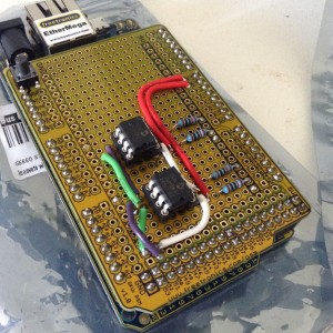
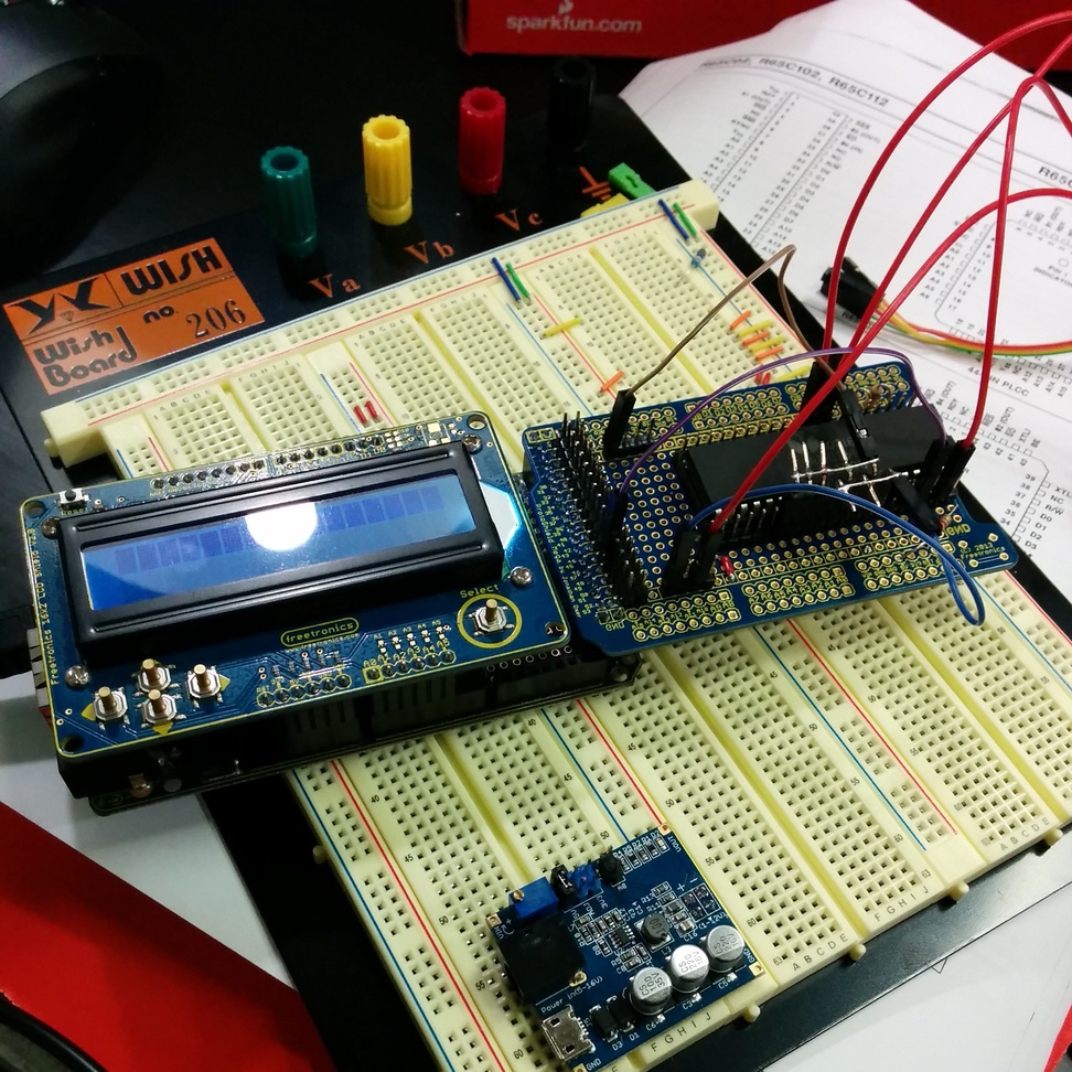
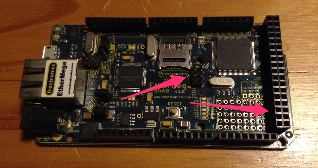
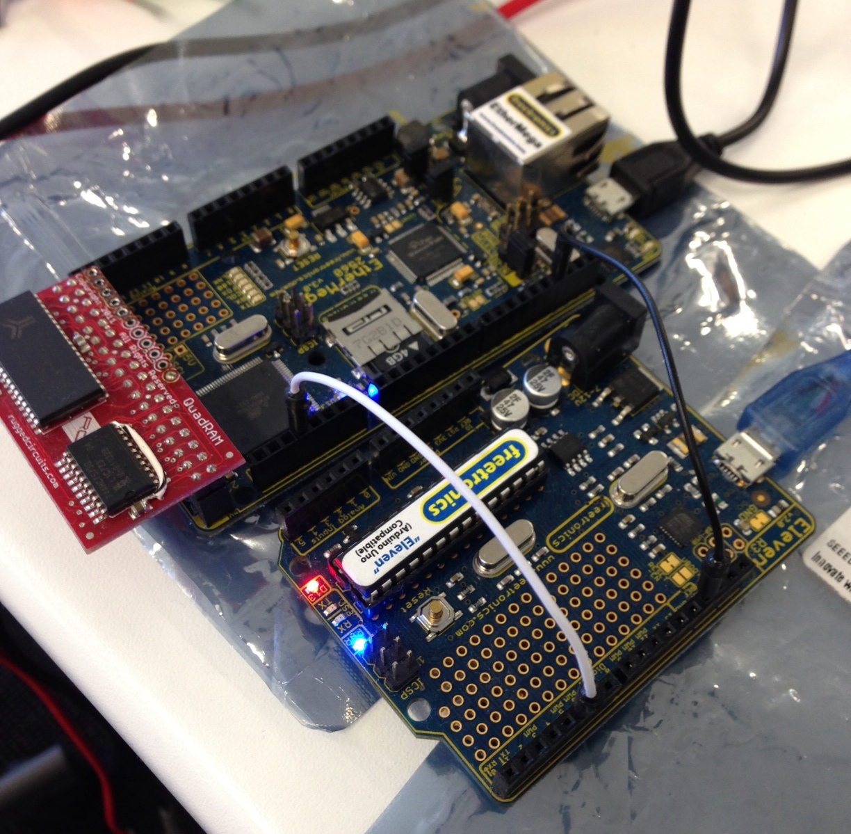
SPI SRAM shield mounted on an Freetronics Ethermega

In my previous post I had figured out that I could capture memory accesses in my simulator and send them elsewhere.

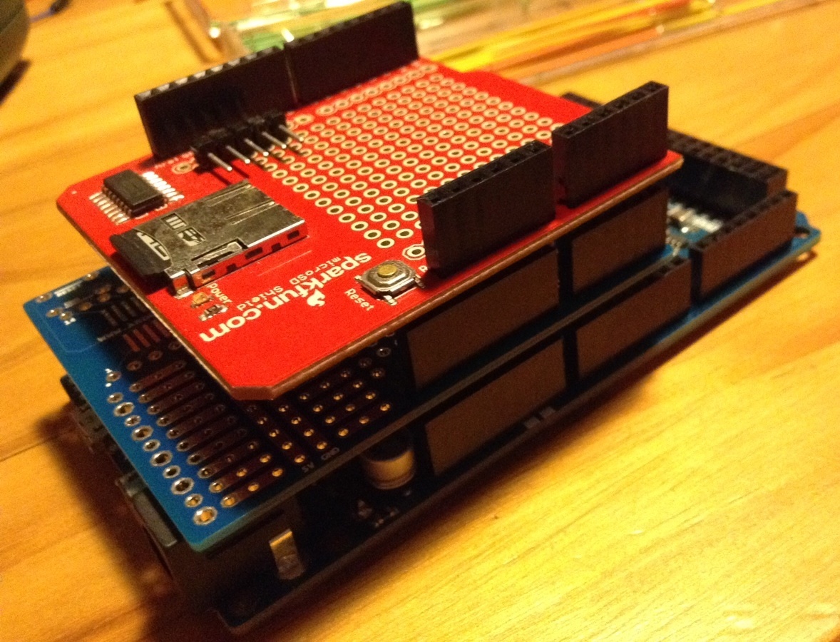
In version 1 of the design I (ab)used the onboard mini SD card to simulate the entire address space. This was a very 1950’s solution and came with matching performance.

Still, it did give me confidence that this project was possible and so I located a kit which would give me a better performing memory subsystem. I duly ordered the kit from Colin Irwin but didn’t know how long it would take to get here from France.

Trolling around eBay I had found various EEPROM solutions like this one which I thought I could adapt. The board wasn’t directly usable as it was configured for 2 wire I2C, not 3 wire SPI, but it suggested to me that I could build a shield to hold some SRAM chips to get my project going while I waited for the XRam shield to arrive.

There is a common SRAM chip, the Microchip 23K256, which is a 32 kilobyte chip with an SPI interface. I’ve seen it used in various PIC designs, and is an option on the Propeller PMC.

The 23K256 isn’t as common in Arduino designs because of one major flaw; it’s a 3v3 part. This would mean adding a level converter to the shield and being careful not to drop 5 volts across any of the pins on the chip.

There was also the problem of capacity. To get to 256 kilobytes I would need 8 chips on the same SPI bus, and a logic level converter, not counting the onboard SPI devices like the micro SD card and the Wiznet ethernet chip that come with the Ethermega. This was likely to get more complicated than I was planning on, so I continued to look for an alternative SRAM part.

Version 2, the 23LC1024

Luckily I didn’t have to look very far. The Microchip 23LC1024 has 4 times the capacity, and can operate at 5 volts. This meant I would only need two chips to get 256kb and would only need to dedicate two pins to driving the Chip Select lines on the SRAM ICs.

As I live in Australia, there is a difference between choosing the part you want, and actually being able to buy it. While most of the Microchip stock appeared to be in the UK, I found the last two chips in stock at a Element 14, and ordered them straight away. Spares? Pfft, those are for people with no self confidence.

breadboardin

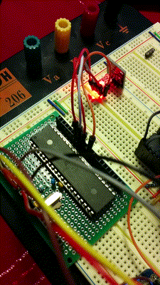
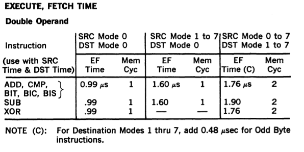
wow. such unstable. so noise. very breadboard

Spelunking on the Arduino forums had yielded some war stories and a nice SpiSRAM library to interface with the chips. It also came with a small ram test sketch.

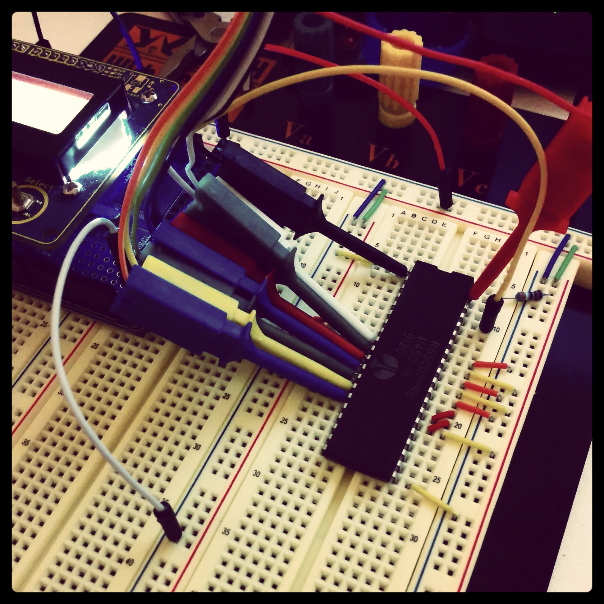
My first attempts to integrate the 23LC1024s on the breadboard wasn’t very successful. Even though I follow the application note I wasn’t able to get the chips to reliably pass the SRAM test. Sometimes the data would be written perfectly, other times it would just be garbage.

By default the 16Mhz Atmel parts drive the SPI pins at 4Mhz. From reading other blogs it was clear that this sort of frequency is outside what the breadboard is designed for, not to mention the large patch leads between the Ethermega and the breadboard.

Increasing the SPI divider to slow down the transactions sort of worked, but it was clear I wouldn’t be able to hook the SRAM up to the avr11 in this condition so I’d need to build a proper shield to hold the ICs.

closeup

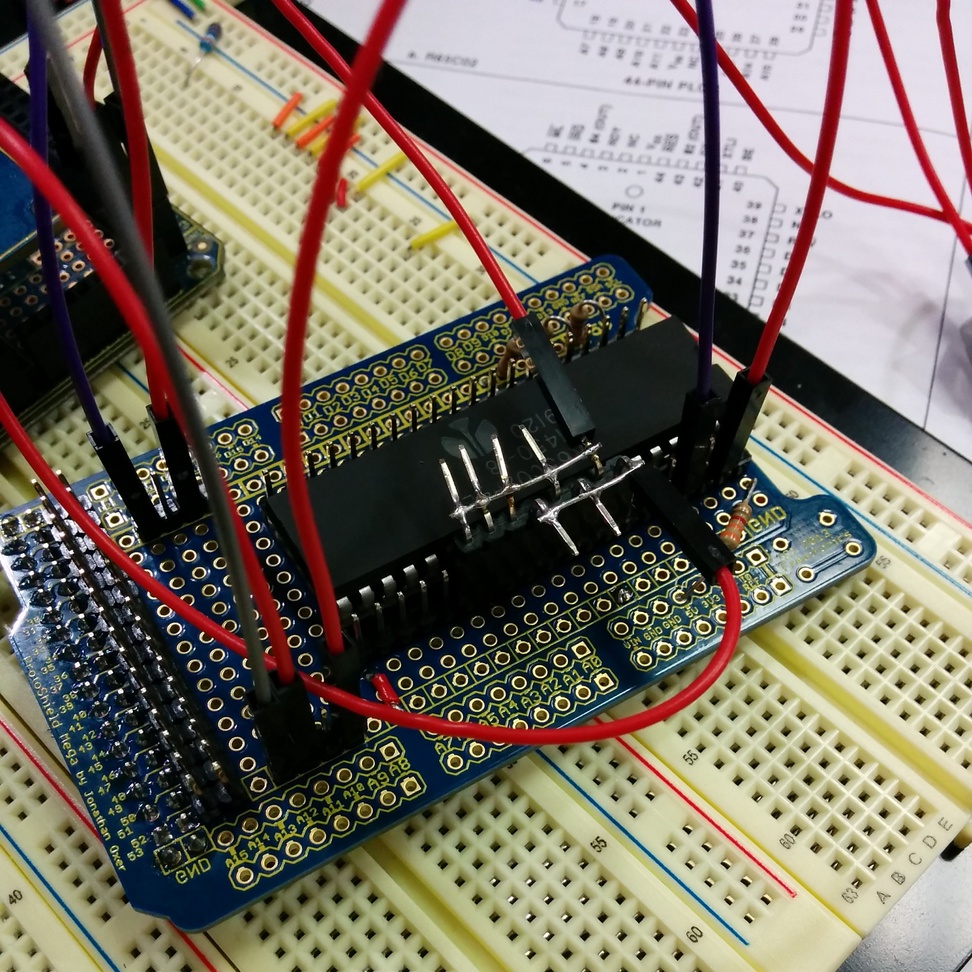
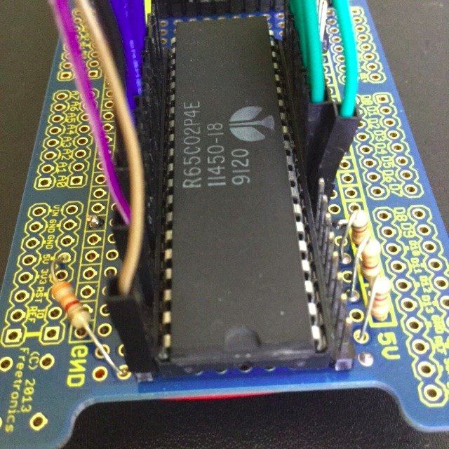
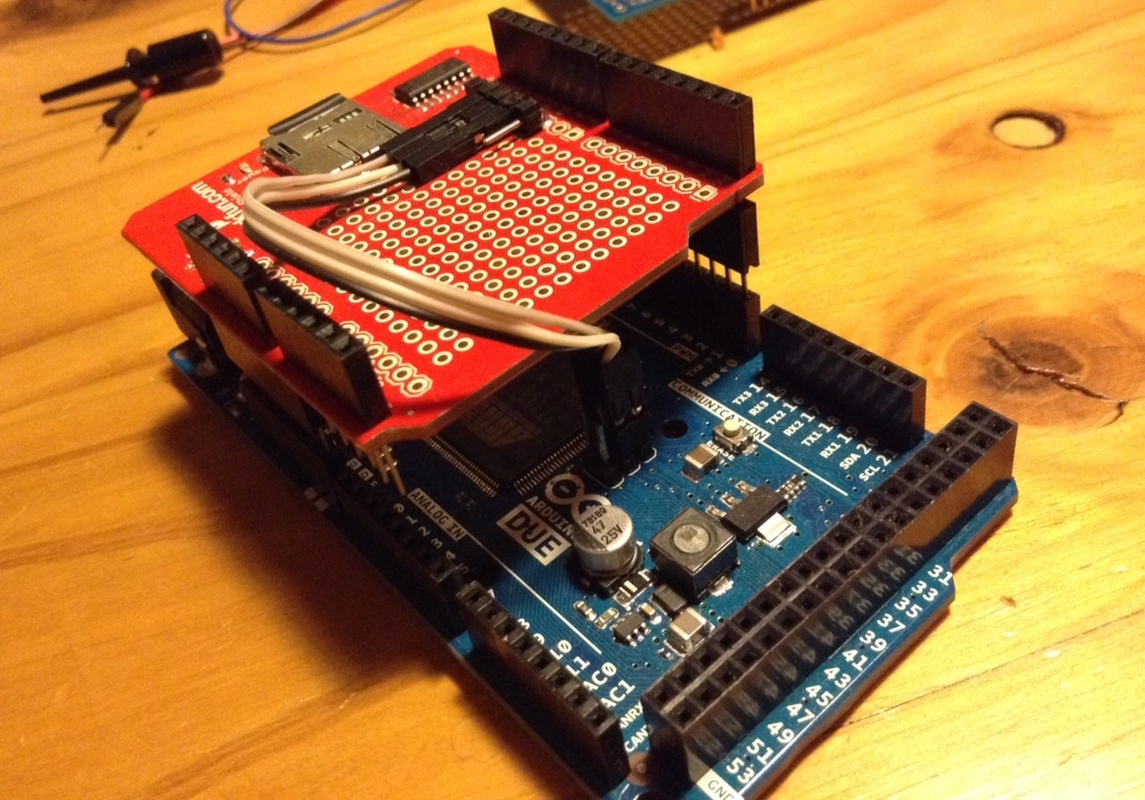
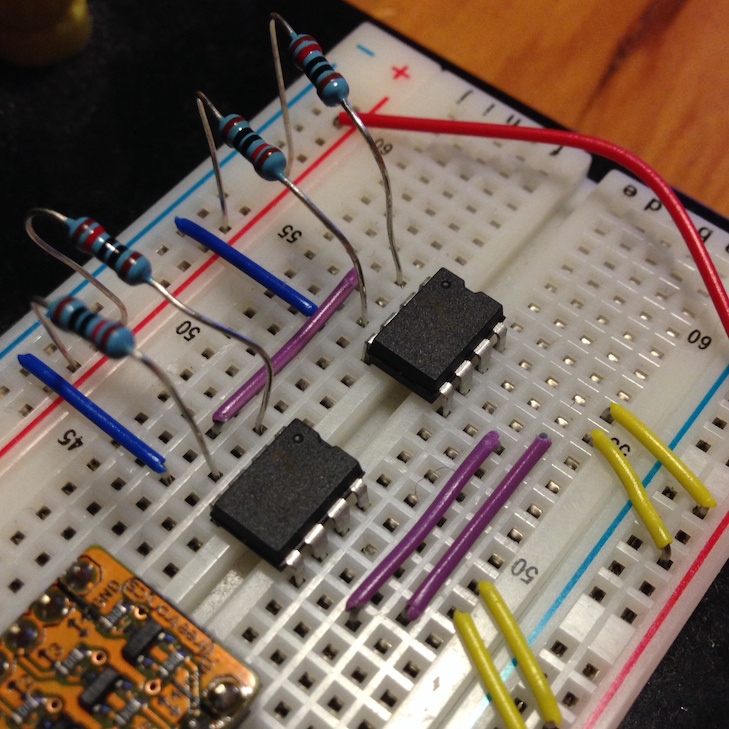
Closeup of the shield. No, you may not see the under-side.

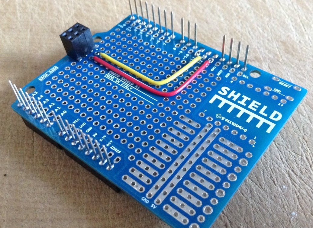
A few days and another trip to Jaycar later, I had all the parts I needed. A few hours bodging at the local hacker space and I had reproduced my design onto a prototyping shield allocating pins D6 and D7 as the chip select pins.

I took the shield home, plugged in the chips and both banks worked first time! Getting cocky I loaded the avr11 sketch and discovered that the micro SD card had failed to initialise, WTF! Reloading the sketch, the SD card worked fine, but the SRAM test showed garbage.

The source of the problem turned out to be the default state of the digital pins on the Arduino. The way SPI works is all the components on the SPI bus share three lines, MISO (master in, slave out), MOSI (master out, slave in), and SCLK (a clock line driven by the master). Additionally every device has its own Chip Select line which must be held high to inhibit the device unless you want to talk to it.

To talk to an individual device, you lower the CS line connected to that chip and read and write data on MOSI/MISO, toggling the SCLK line. All the other devices which have their CS lines high are supposed to hold their MISO and MOSI at a high impedance and ignore transactions on the bus.

The problem is, when the Arduino resets, all the digital lines are set to input and are low; you don’t want an Arduino with no sketch loaded suddenly sending 5volts out of every digital pin. In effect all the Chip Select lines could be active, meaning all the components are listening to the transaction and trying to interact with the master.

The solution I came up with was to ensure that all the digital pins are set to output and held high before calling any of the SD.begin() or SPI.begin() functions.

void setup(void) {
  // setup all the SPI pins, ensure all the devices are deselected
  pinMode(4, OUTPUT); digitalWrite(4, HIGH);    // micro sd
  pinMode(6, OUTPUT); digitalWrite(6, HIGH);    // bank0
  pinMode(7, OUTPUT); digitalWrite(7, HIGH);    // bank1
  pinMode(10, OUTPUT); digitalWrite(10, HIGH);  // wiznet
  pinMode(53, OUTPUT); digitalWrite(53, HIGH);  // atmega2560 SS line
  ... more setup code

In effect this disables all the SPI devices until their various begin() functions were called to configure them.

Maybe this wasn’t the best solution, but since I implemented it the SRAM and SD card have been perfectly stable so I consider it case closed.

Coming up

This post takes me up to the present day. Right now I have a XRam kit to be built up, and a QuadRAM which was sold to me by a very kind blogger who wasn’t using it, sitting on my desk.

Both the XRam and QuadRAM are functionally identical and each can provide more that the 256kb of SRAM needed for this project which is effectively directly integrated into the atmega2560’s address space.