Monthly Archives: January 2014

avr11: profiling on the Atmega

This is a post about the performance of my avr11 simulator. Specifically about the performance improvements I’ve made since my first post, and the surprises I’ve encountered during the process.

Old school profiling

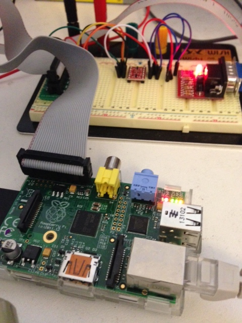
Because avr11 runs directly on the Atmega 2560 microcontroller, there is no simple way to measure the performance of various pieces of code externally.

I am aware that Atmel studio contains a fairly accurate simulator, but that package only runs on Windows. It also wasn’t clear if it can simulate the microSD card and xmem boards that avr11 requires. That left me needing to improvise some way of measuring the relative performance of avr11 while I made changes to the code.

The solution I came up with was a counter that increments every time cpu::step(), the function that processes one instruction, is called. The counter is defined as uint16_t so rolls over every 2^16 instructions. Combined with the built in millis() function, which prints the number of milliseconds since reset, I had a crude way of timing how long avr11 takes to dispatch instructions.

    cpu::step();
    if (INSTR_TIMING && (++instcounter == 0)) {
      Serial.println(millis());
    }

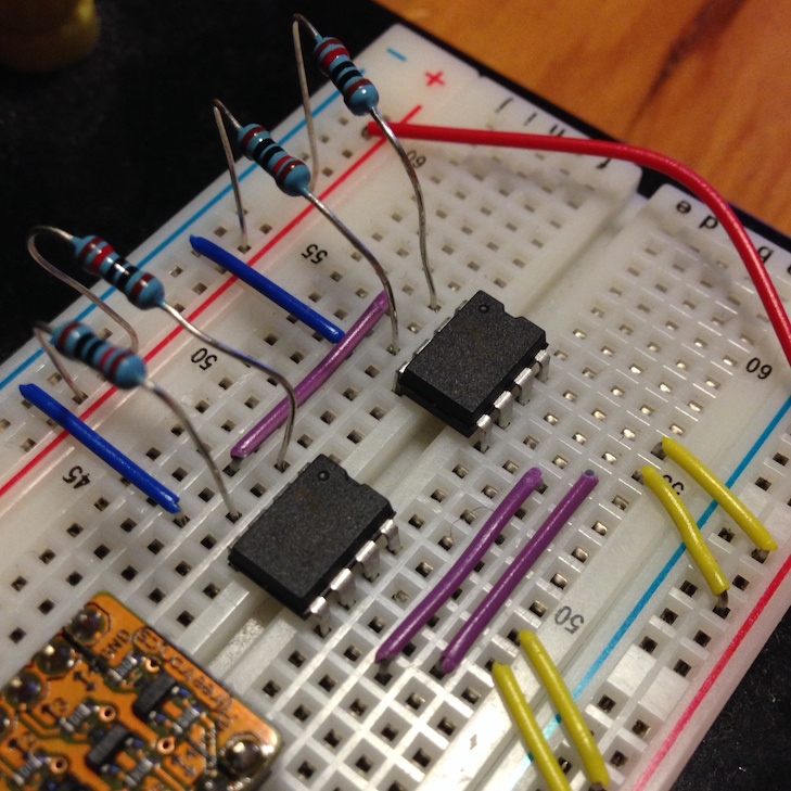
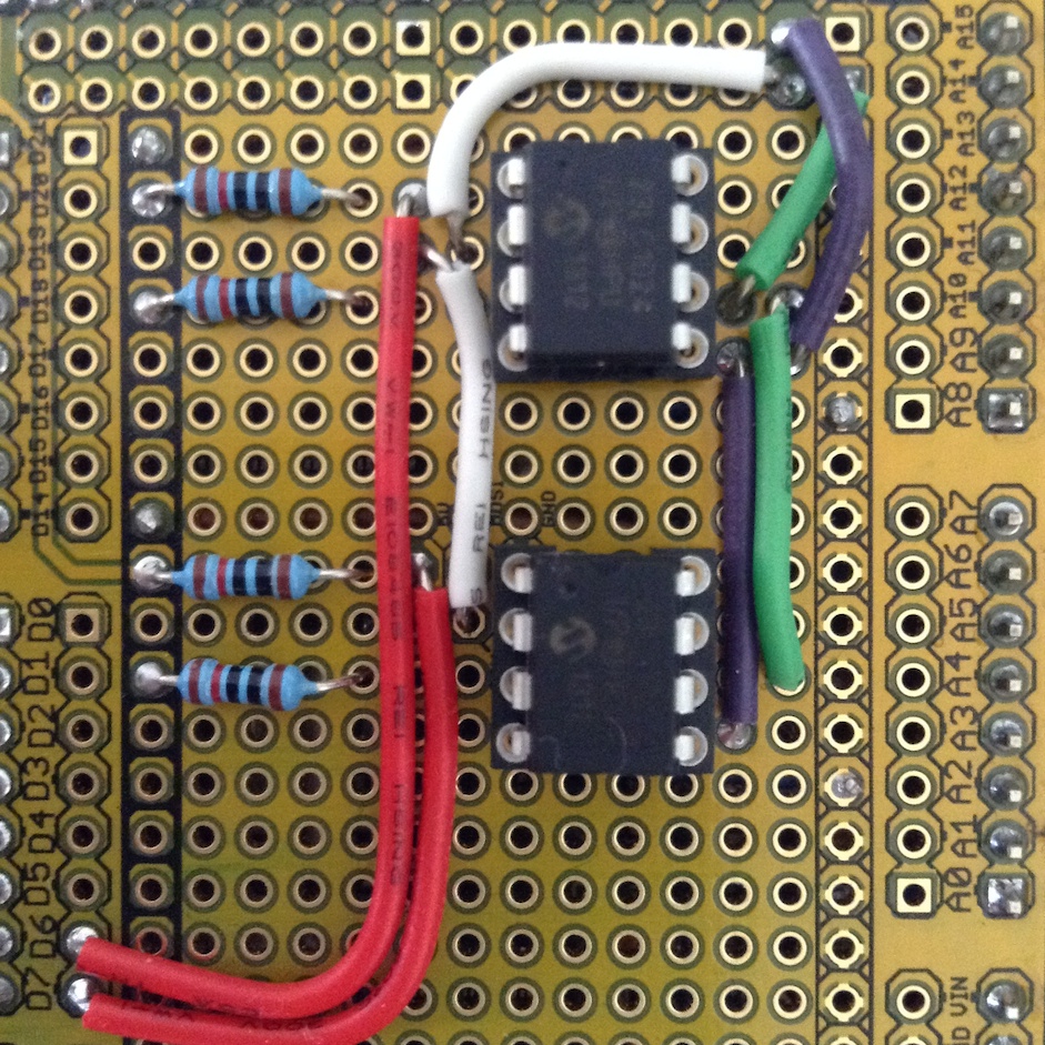
From there the process became very iterative. Each evening I would spend a few hours playing with various tweaks in the Go version of avr11, then I would transpose them over to the C++ code a piece at a time, testing as I went and watching the cycle count.

Some promising results

TL;DR – Instruction dispatch was an average of 144 microseconds with the mmu disabled1, 160 with the mmu enabled. It is now 60 microseconds with the mmu disabled, and a few microseconds more with the mmu enabled. 2.4x improvement.

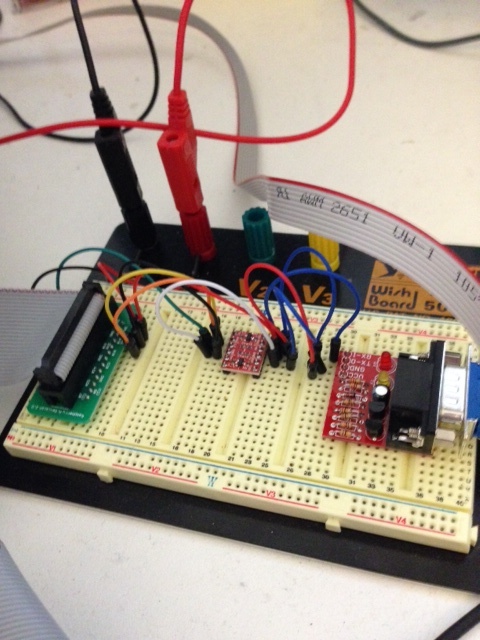
The first big improvement came from switching from the Arduino SD classes to the SdFat library. SdFat gives you more control over the interactions with the card, and also lets you set the speed of the SPI bus, on 16 Mhz Atmels, to full speed, rather then the previous 1/2 speed maximum. This gave me an 8-10% improvement in memory access times to the SPI SRAM shield.

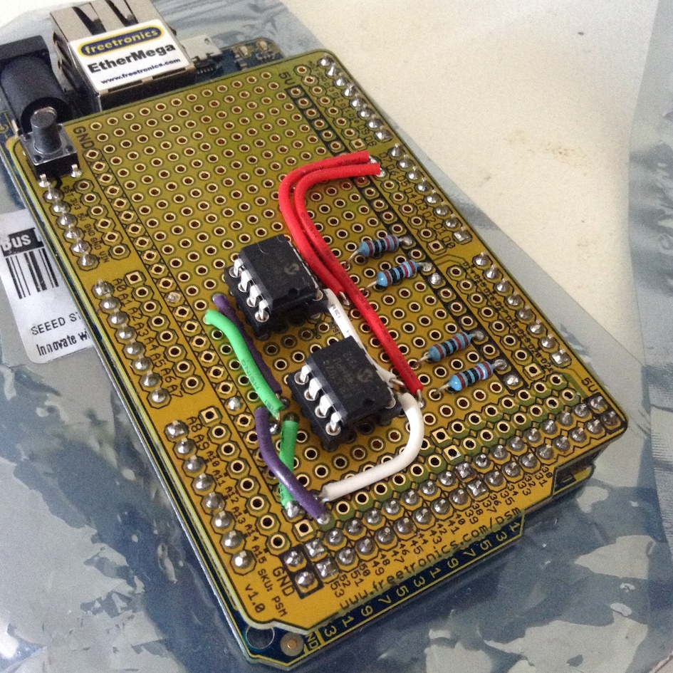
The next big improvement came from switching from the SPI SRAM shield to a Rugged Circuits’ QuadRAM board. This eliminates the SPI bus entirely by extending the address space of the Atmega 2560 to the full 64 kilobytes and adding banking to access up to 512 kilobytes. This gave another 20% improvement.

After that things got harder. The remaining 30 microsecond improvements came from careful rewriting of all the hot paths and reducing the data types involved to their smallest possible type.

A surprising discovery

The most surprising discovery of all was made as I started to comment out pieces of the code to get a baseline for the inner loop of the simulator.

After whittling it down to simply fetching the instruction at the current PC I’d arrived at a baseline of 21 microseconds. That is just under 50 kilohertz simulated performance; not great, especially considering this isn’t processing the instruction.

Digging a little further I discovered that this one shift to set the correct memory bank costs 4-5 microseconds. Out of a total time of 21 microseconds, that is close to 25% in just one line.

  if (a < 0760000 ) {     
    // a >> 15 costs nearly 5 usec !!
    uint8_t bank = a >> 15;
    xmem::setMemoryBank(bank, false);
    return intptr[(a & 0x7fff) >> 1];
  }

In retrospect this shouldn’t have been a surprise. The Atmega processor is an 8 bit processor. It has some provisions for 16 bit quantities, but they are expensive. 32 bit quantities probably receive no hardware support, and I think in this instance avr-gcc is calling a helper function for the unaligned shift.

A quick hack using a cast and some shifts shaved 4 microseconds off the inner loop, clearly attributable to this inefficient shift. The proper fix will probably involve more radical surgery using a union datatype.

Conclusion

If this post has a moral, it would have to be

Don’t guess, always profile your code.

As for the performance of avr11, it stands a 16 kilohertz simulated clock speed. Possibly with some extreme C surgery this can be improved to 20 kilohertz. Past that, the possibilities running on the Atmega 2560 look grim.

I’d be interested in hearing from other Atmel users about their profiling methods.


  1. The PDP-11/40 I am simulating has an 18 bit address space. However the CPU is only 16 bit and cannot directly generate 18 bit addresses so a memory management unit is used to rewrite addresses as they leave for the UNIBUS. The MMU adds a small overhead to memory reads and writes when enabled. In the original hardware that was somewhere on the order of 90 nanoseconds. In simulation it’s probably under 5 microseconds.

avr11: building an SPI SRAM shield for an Arduino Mega

spi-sram-shield

SPI SRAM shield mounted on an Freetronics Ethermega

In my previous post I had figured out that I could capture memory accesses in my simulator and send them elsewhere.

In version 1 of the design I (ab)used the onboard mini SD card to simulate the entire address space. This was a very 1950’s solution and came with matching performance.

Still, it did give me confidence that this project was possible and so I located a kit which would give me a better performing memory subsystem. I duly ordered the kit from Colin Irwin but didn’t know how long it would take to get here from France.

Trolling around eBay I had found various EEPROM solutions like this one which I thought I could adapt. The board wasn’t directly usable as it was configured for 2 wire I2C, not 3 wire SPI, but it suggested to me that I could build a shield to hold some SRAM chips to get my project going while I waited for the XRam shield to arrive.

There is a common SRAM chip, the Microchip 23K256, which is a 32 kilobyte chip with an SPI interface. I’ve seen it used in various PIC designs, and is an option on the Propeller PMC.

The 23K256 isn’t as common in Arduino designs because of one major flaw; it’s a 3v3 part. This would mean adding a level converter to the shield and being careful not to drop 5 volts across any of the pins on the chip.

There was also the problem of capacity. To get to 256 kilobytes I would need 8 chips on the same SPI bus, and a logic level converter, not counting the onboard SPI devices like the micro SD card and the Wiznet ethernet chip that come with the Ethermega. This was likely to get more complicated than I was planning on, so I continued to look for an alternative SRAM part.

Version 2, the 23LC1024

Luckily I didn’t have to look very far. The Microchip 23LC1024 has 4 times the capacity, and can operate at 5 volts. This meant I would only need two chips to get 256kb and would only need to dedicate two pins to driving the Chip Select lines on the SRAM ICs.

As I live in Australia, there is a difference between choosing the part you want, and actually being able to buy it. While most of the Microchip stock appeared to be in the UK, I found the last two chips in stock at a Element 14, and ordered them straight away. Spares? Pfft, those are for people with no self confidence.

breadboardin

wow. such unstable. so noise. very breadboard

Spelunking on the Arduino forums had yielded some war stories and a nice SpiSRAM library to interface with the chips. It also came with a small ram test sketch.

My first attempts to integrate the 23LC1024s on the breadboard wasn’t very successful. Even though I follow the application note I wasn’t able to get the chips to reliably pass the SRAM test. Sometimes the data would be written perfectly, other times it would just be garbage.

By default the 16Mhz Atmel parts drive the SPI pins at 4Mhz. From reading other blogs it was clear that this sort of frequency is outside what the breadboard is designed for, not to mention the large patch leads between the Ethermega and the breadboard.

Increasing the SPI divider to slow down the transactions sort of worked, but it was clear I wouldn’t be able to hook the SRAM up to the avr11 in this condition so I’d need to build a proper shield to hold the ICs.

closeup

Closeup of the shield. No, you may not see the under-side.

A few days and another trip to Jaycar later, I had all the parts I needed. A few hours bodging at the local hacker space and I had reproduced my design onto a prototyping shield allocating pins D6 and D7 as the chip select pins.

I took the shield home, plugged in the chips and both banks worked first time! Getting cocky I loaded the avr11 sketch and discovered that the micro SD card had failed to initialise, WTF! Reloading the sketch, the SD card worked fine, but the SRAM test showed garbage.

The source of the problem turned out to be the default state of the digital pins on the Arduino. The way SPI works is all the components on the SPI bus share three lines, MISO (master in, slave out), MOSI (master out, slave in), and SCLK (a clock line driven by the master). Additionally every device has its own Chip Select line which must be held high to inhibit the device unless you want to talk to it.

To talk to an individual device, you lower the CS line connected to that chip and read and write data on MOSI/MISO, toggling the SCLK line. All the other devices which have their CS lines high are supposed to hold their MISO and MOSI at a high impedance and ignore transactions on the bus.

The problem is, when the Arduino resets, all the digital lines are set to input and are low; you don’t want an Arduino with no sketch loaded suddenly sending 5volts out of every digital pin. In effect all the Chip Select lines could be active, meaning all the components are listening to the transaction and trying to interact with the master.

The solution I came up with was to ensure that all the digital pins are set to output and held high before calling any of the SD.begin() or SPI.begin() functions.

void setup(void) {
  // setup all the SPI pins, ensure all the devices are deselected
  pinMode(4, OUTPUT); digitalWrite(4, HIGH);    // micro sd
  pinMode(6, OUTPUT); digitalWrite(6, HIGH);    // bank0
  pinMode(7, OUTPUT); digitalWrite(7, HIGH);    // bank1
  pinMode(10, OUTPUT); digitalWrite(10, HIGH);  // wiznet
  pinMode(53, OUTPUT); digitalWrite(53, HIGH);  // atmega2560 SS line
  ... more setup code

In effect this disables all the SPI devices until their various begin() functions were called to configure them.

Maybe this wasn’t the best solution, but since I implemented it the SRAM and SD card have been perfectly stable so I consider it case closed.

Coming up

This post takes me up to the present day. Right now I have a XRam kit to be built up, and a QuadRAM which was sold to me by a very kind blogger who wasn’t using it, sitting on my desk.

Both the XRam and QuadRAM are functionally identical and each can provide more that the 256kb of SRAM needed for this project which is effectively directly integrated into the atmega2560’s address space.

avr11: how to add 256 kilobytes of ram to an Arduino

18 bits of core memory

In Schmidt’s original javascript simulator, and my port to Go, the 128 kilowords (256 kilobytes) of memory connected to the PDP-11 is modeled using an array. This is a very common technique as most simulators execute on machines that have many more resources than the machines they impersonate.

However, when I started to port my Go based simulator to the Arduino, the problem I faced was the Atmel does not support an address space larger than 64 kilobytes, and more immediate, all the 8 bit Atmega models ship with somewhere between 2kb and 8kb of addressable memory.

Version 0, use the Arduino itself

Deciding to put that problem to the side until I saw if the job of rewriting (and dusting off my long obsolete C coding skills) was achievable, the first version of the simulator I wrote did use a simple array for UNIBUS memory.

#define MEMSIZE 2048
uint16_t memory[MEMSIZE];

Using an Atmega2560 I was able to create a memory of 4096 bytes, which was enough to bring up the simulator and run the short 29 word bootstrap program which loaded the V6 Unix bootloader into memory.

Sadly the bootloader would fault the simulated CPU almost immediately as the first thing the bootloader does is zero the entire address space, quickly running past the end of the array and overwriting something important.1

However, this did let me get to the point that the CPU and RK11 drive simulators were working well, not to mention figuring out how to write a large multi file program using the Arduino IDE environment.

Memory lives somewhere else

A revelation I have recently arrived at is that, from the point of view of a CPU, memory is not part of the processor. Data in a real CPU moves into and out of the device in a very orchestrated manner and in avr11 this is no different.

Any instruction that references memory, either directly loading data into a register via the MOV instruction, or indirectly using one of the PDP-11’s addressing modes always boiled down to a read or write function which linked the CPU to the simulated UNIBUS.

For example, in the Go version of the simulator, memory []uint16 belongs to the unibus struct. In the C++ version for Atmel this is enforced further by there being no extern uint16_t memory[MEMSIZE]; definition exposed in unibus.h.

In short, there is no way for the CPU to observe memory, it has to ask the UNIBUS to read or write data on its behalf, and this gave me the opportunity to solve the problem of limited memory space available on the Atmel devices I had access to.

Version 1, I am a bad person

At this point I’m sort of telling the story backwards. I had found a product which would give me far more memory than I needed for this project, but it took several weeks to arrive and comes as a kit, which will involve some tricky SMD soldering.

In the interim I found myself during the Christmas to New Years break with a simulator that I felt was working well enough to try something more adventurous if I could only find some way to emulate the backing array for the core memory. I didn’t really care about speed, I just wanted to see if the simulator could handle the more complicated instructions of the Unix kernel.

“Why not use the SD card?” I said to myself. I was after all already loading some of the blocks off the RK05 disk pack image from the card, so why not just make another image file and make that back the core memory. The mini SD card probably wouldn’t last very long, but I have a pile of cheap cards so why not try it.

 void pdp11::unibus::write8(uint32_t a, uint16_t v) {
    if (a < 0760000) {
       if (a & 1) {
         core.seek(a);
         core.write(v & 0xff);
         //memory[a >> 1] &= 0xFF;
         //memory[a >> 1] |= v & 0xFF << 8;

All it took was setting up a new SD::File, called core and rewriting the access to the memory array with seeks and writes to the backing file (obviously doing the same for the read paths).

Amazingly it worked, on the second or third attempt, and although it was very slow I was able to use this technique to boot the simulator a very long way into the Unix boot process. I posted a video of the bootup to instagram.

Even more amazingly I didn’t wear out the mini SD card, and still haven’t. This is probably mostly due to the wear leveling built into the card2 but I also stumbled into a fortuitous property of the SD card itself, and the Arduino drivers on top.

All SD cards, well certainly SD and mini SD cards, mandate that you read and write to them in units of pages. Pages happen to be 512 bytes, a unit which clearly descends from the days of CF cards which emulated IDE drives.

This means the Arduino SD class maintains a buffer of 512 bytes, (which comes out of your precious SRAM allotment) that in effect operated as a cache for my horrible all swap based memory system. For example, when the bootloader program zeros all the memory in the machine, rather than writing to the SD card 253,952 times3, the number of writes was probably much smaller, say 500 writes.

Obviously as it was not designed for this purpose the cache would fail badly during a later part of the bootup where the kernel code is copied (about 90 kilowords of it) from one memory area to another. Each read or write would land on a different SD card page, causing it to flush the old buffer, read in the new buffer, then reverse the process.

But it worked, and gave me confidence to investigate some more ambitious designs for a memory solution.

In my next blog post I’ll talk about version 2 of my memory system, the one that I finally got me booting to the # prompt.


  1. I considered using a SAM3X atmel32 style board, like the Arduino Due as they have both a more powerful CPU and close to 96 kilobytes of addressable memory, but that is only 48 kilowords, less than half of what I need to simulate the full 128 kiloword address space of the PDP-11.
  2. The internet is divided on the question of “Do cheap mini SD cards have wear leveling?”. Part of the problem is the definition of cheap changes rapidly over time, making advice written 12 months ago inaccurate. My view is that cards of any capacity you can buy today require so much error correction logic that you get the wear leveling logic for free.
  3. On the PDP the top 4 kilo words of memory (8kb) is reserved for the IO devices, so while the UNIBUS talks in 18 bit addresses, the top 4096 words is not mapped to memory, and doesn’t need to be cleared. In fact clearing the IO page memory would be catastrophic.

avr11: simulating minicomputers on microcontrollers

Introduction

The avr11, a atmega2560 clone with a custom SPI 256kb memory.

The avr11, an atmega2560 clone with a custom SPI 256kb memory.

It all started with Javascript.

In April of 2011 Julius Schmidt wrote a PDP-11 emulator that ran in a browser. I thought that this was one of the most amazing thing I had ever seen.

Late last year I ran across the link again in my Pocket backlog and spent a little time poking around the code that powered the simulator.

The PDP-11 architecture is very interesting. All the the major system components work asynchronously, co-ordinating access via the shared UNIBUS backplane. Julius’ simulator used this property and callbacks on timers to simulate components like the disk and console operating asynchronously.

I’ve written previously about the suitability of Go for writing emulators and so I thought it would be a fun project to port Julius’ work to Go. This port is going well and provided the base for porting the code to C++ for this project.

Around the same time I ran across several other projects which convinced me to try an Atmel port.

The first was the winner of last years IOCCC, a 4k Intel 8086 simulator1 which showed me that the core of a CPU simulator could be small. Ignoring main memory, you need only simulate the small number of registers defined by the architecture. The PDP-11 has 8 16bit registers, a few service registers and 32 16 bit mmu registers2 to hold mappings. This would fit even in a small microcontroller like the 328p or 32u4.

The second project was a hardware implementation of a 32bit ARM CPU running linux on an Atmel 128p. Probably built as a dare, this project showed me that reliable simulators can be built on the 8bit Atmel platform and an external device could be used to represent the larger main memory expected by the CPU being simulated.

Maybe this wasn’t as crazy as it sounded.

Why the PDP-11 ?

PDP11/45 console. Image courtesy of John Holden's PDP11 page.

PDP-11/45 console. Image courtesy of John Holden’s PDP-11 page.

The PDP-11 is the most important minicomputer of the 1970’s.

The cost of the PDP-11 was low enough that it could be dedicated to one person or small group when mainframe computers cost so much to run that time was billed by the hour to recoup their phenomenal cost. DEC machines quickly became the platform for research and experimentation.

The PDP-11 was the machine that Ken Thompson and Dennis Ritchie developed Unix and the C programming language. As a historical artefact it has tremendous importance for anyone who is interested in computer programming or retro computing.

If you want to know why the int datatype in C defaults to 16 bits, look at the PDP-11, it was a 16 bit computer. If you want to know why a char is called a char not a byte look to way the PDP-11 stored two characters in a word.

So, what better way to learn about the PDP-11, and the history of C and Unix, than to build a simulator of the machine that started it all ?

Why build a simulator on a microcontroller?

Let’s be honest, the world doesn’t need another Arduino weather station.

Apart from wiring up LED and LCD displays I haven’t really found anything that really excites me about using microcontrollers. In some ways, the way that microcontrollers are coded and used feels very batch oriented — write some code, compile it, load it onto the micro, wait quietly to see it it worked, rinse, repeat.

I had heard a Podcast interview with one of the makers of the Pebble smart watch and learnt about the Pebble OS, a fork of FreeRTOS.

FreeRTOS looked like as a way to write interactive programs on microcontrollers, and those ideas were percolating inside my head while I was porting Julius’ Javascript simulator to Go over Christmas.

One of the nice features of Julius’ simulator was the very clean separation between the CPU logic and the memory logic. In the PDP-11 memory is just another device on the UNIBUS bus and so I began to think that if I could find some way of connecting the required 128 kilowords of memory to an Atmel the rest of the simulator should fit within the onboard SRAM.

What works today

A screenshot of one of the first successful boot attempts.

A screenshot of one of the first successful boot attempts.

Today the simulator boots V6 unix and can execute some simple commands, there are some remaining bugs in the mmu which cause the simulator to fail when larger programs (/usr/bin/cc and /usr/games/chess for example) are executed

The hardware emulated is somewhere between a PDP11/40 and PDP11/45. The EIS option (MUL and DIV) is properly emulated, but FIS (floating point is not).

Only a single RK05 drive is simulated, backed by a file on the micro SD card.

I want to improve the accuracy of the simulator so that it can run V7 unix, 2.9/2.11 BSD, RSX-11M and most importantly, the DEC diagnostics.

All these improvements are first developed on the Go port then will be integrated into the Atmel port.

How is the performance?

Right now, not great. I don’t have a real PDP-11 for comparison, but looking at some videos on Youtube I’d have to say the simulator is at least 10x slower than an original 11/40.

I was never expecting to be amazed with the speed of this simulator, especially at this early stage. However, on a performance per watt basis, I think it’s hard to beat avr11.

The PDP-11 that this simulator models is spartan, even by the standards of the early 70s, yet still consumed over 2 kilowatts of power for the CPU and Memory (256kb). The 2.5 megabyte RK05 boot drive was another 600 watts. Real unix installations would have 3 or more drives, so there goes another 1200-1800 watts.

Compared to that, the avr11 draws well under the 500ma limit of a USB port. Although I lack equipment to measure the current draw I estimate it to be around 100ma at 5 volts which is 0.5 watts. Tell that to your data center manager.

Some specific performance issues I am aware of are:

  1. 32 bit register operands. Everything in the CPU is treated as a 32 bit integer during the simulation of the individual instructions. This is a hold over from the original Javascript simulation. The Atmel is internally an 8 bit CPU. There are provisions for 16 bit, double byte operations, but they come at a cost of 5x over their 8 bit counterparts. Using 32 bit operands are even more costly again.
  2. SPI memory. The overhead of the SPI transaction to read a word from memory is quite high. As most instructions generate at least 2 memory cycles, and can be as high as 6, fetching operands from memory consumes a lot of wall time.

Getting the code

Julius’ original Javascript implementation, from which both my Go and Atmel ports derive, is licensed under the liberal WTFPL licence. As I share similar views on software licensing, both of my projects will be similarly licensed.

The code itself is on Github. As of today it is frankly a dog’s breakfast of babies first C++ programming and Arduino hacks. As the project progresses I hope this will improve.

Ethermega and SPI SRAM shield.

Ethermega and SPI SRAM shield (unpopulated).

However the code itself isn’t much use without the hardware. Again this is under heavy flux and I hope to improve the number platforms the simulator can run on.

The specific hardware requirements are an Atmega2560 (the older 1280 will also work, I just don’t have one to experiment with). I’m using the Freetronics Ethermega, mainly because it was what I could buy at Jaycar, but also because it has a built in micro SD card reader onboard.

The SPI SRAM shield is custom, and I’ll be writing about it in my next post.


  1. The author of 8086tiny has recently released a de-obfuscated version of their emulator.
  2. Actually Julius’ emulator cheated, there are actually 3 banks of 16 mmu registers in a real KT11 mmu, but V6 unix doesn’t use supervisor mode, so we can cheat a little here.

What did devops mean ?

This post is a rant about a word. A rant about a word that had a clear meaning but has been appropriated for something wholly less meaningful.

The word is of course Devops. Over the last few years, as the practice itself has grown in prominence, its description has become diluted beyond the point of recovery.

It is far to common place to hear Devops used as a synonym for someone who automates technology, or even just to mean automation. Just as disappointing is the wholesale rebranding of Systems Administration as Devops.

Here is a pro tip: if you’re the only person on the team, or in the company, who carries the pager, it’s not Devops.

You keep using that word, I don’t think it means what you think it means

So what happened ? Where did things go wrong ?

Devops is was an idea, a movement, a set of practices about using technology to deliver shit that you are supposed to deliver not point fingers. But movements are hard to sell, and harder to buy as the term cannot be used to describe succinctly what the person would do.

A systems administrator administers computer systems. A network administrator administers computer networks. A computer programmer programs computers. What does a Devops do again ?

It’s easy to stick the boot into the facile recruiting industry and lay the blame at their door, but it’s not really their fault. At their heart recruiters are sales people, and their goal is to sell you something (or someone) and semantic arguments won’t keep the lights on.

Why exactly is it you are using recruiters ?

In memoriam

If this post is then a eulogy for Devops, what other words can be used instead to describe it ?

If when you say Devops you actually mean Automation then the words you want to use are Infrastructure as Code. As a term and a brand it appears robust against appropriation, and if that is your bag then I suggest you checkout @infracoders.

Alternatively if you meant Devops the movement, then a suggestion is to look to the roots of that movement, to Agile itself. Look for teams that espouse Agile values and you’ll probably find a welcome home.

Using go test, build and install

With one exception, the go command takes arguments in the form of packages.

You can pass the package name(s) explicitly, eg.

go test github.com/hoisie/mustache

or implicitly

cd $GOPATH/src/github.com/hoisie/mustache
go test .

By default, if no arguments are provided go test treats the current directory as a package, so in the second example, go test . is identical in function to

cd $GOPATH/src/github.com/hoisie/mustache
go test

The ability to pass a single file to go {build,test,install} is a degenerate case brought about by go run accepting a single .go file as its argument.

go run should be considered the single exception to the rule outlined above.

A real serial console for your Raspberry Pi

rpi-consoleThis post talks about how I connected my Raspberry Pi to a WYSE 60 terminal.

Voltages

The terminal speaks RS232 level, +/- 12v, but the Pi speaks 3.3v TTL levels so some sort of converter is needed to adapt the signalling levels. A logic level converter won’t work as RS232 signalling needs negative voltages as well.

photo (4)

Fortunately Sparkfun sell a great little kit called the RS232 Shifter Board Kit which converts TTL to RS232 levels.

The picture on the left is the SMD version which comes pre made, I also bought the kit version which I am using to connect the RPi. I believe they are identical in function.

Connectors

photo 1The next issue is connecting the terminal to the level shifter. Luckily because the WYSE terminal is hard wired to be a DTE, the RPi falls naturally into its role as a DCE. What does this mean ? It means I didn’t need to build a null modem cable, a short cable to extend the DB9 connector around to the back of the terminal (where I have a DB-9 to DB-25 adapter) was all that was necessary.

A quick trip to Jaycar and I had a few feet of ribbon cable and some DB-9 ribbon cable connectors. Just match up pin 1 on both ends then hammer the plastic bracket to crimp the ribbon cable into the housing.

Wiring

photo 3The image on the left shows how I wired up the RS232 converter to my Pi.

The Pi is connected via a ribbon cable on the P1 header to a breakout connector which lets me plug it into a breadboard.

photo 3In the image on the right you can see the breakout board which lets me tap into the various pins on the P1 header easily.

I’m also providing power to the Pi over the P1 header via the breadboard and my Dangerous Prototypes ATX breakout board.

Between the RS232 converter and the Pi is a level shifter which is translating 3.3v TTL levels from the TX and RX pins to 5v. In theory this shouldn’t be necessary as the RS232 converter is supposed to be able to handle voltages as low as 2.8v but is really designed for interfacing with Arduinos, so shifting the RX and TX signals up to 5v couldn’t hurt.

Setting up the Pi

On last issue to overcome was the Pi by default runs the console at 115,200 baud while the WYSE terminal maxes out at 19,200. To set the operating baud for the console device to be 19,200 baud, you need to edit these two files

  • /boot/cmdline.txt, update the two references to 115200 to 19200.
    dwc_otg.lpm_enable=0 console=ttyAMA0,19200 kgdboc=ttyAMA0,19200 console=tty1 root=/dev/mmcblk0p2 rootfstype=ext4 elevator=deadline rootwait
  • /etc/inittab, updating the line at the bottom, referencing ttyAMA0 to also be 19200.
    #Spawn a getty on Raspberry Pi serial line
    T0:23:respawn:/sbin/getty -L ttyAMA0 19200 vt100

And that is it. Hook everything up and reboot.

Console in action

photo 2I posted a short video of the RPi booting up on instragram.

So, why would you want to do this when PL2303 serial to USB adapters are cheap and available? Well, there is no good reason, apart from it was there, and I had the parts.