Introduction

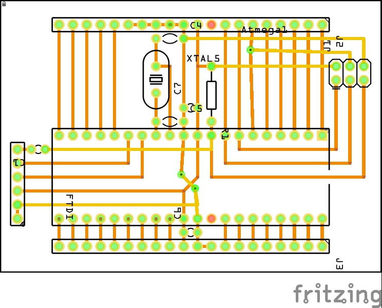
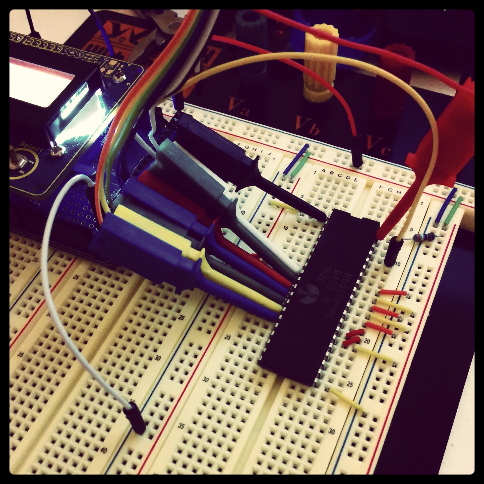
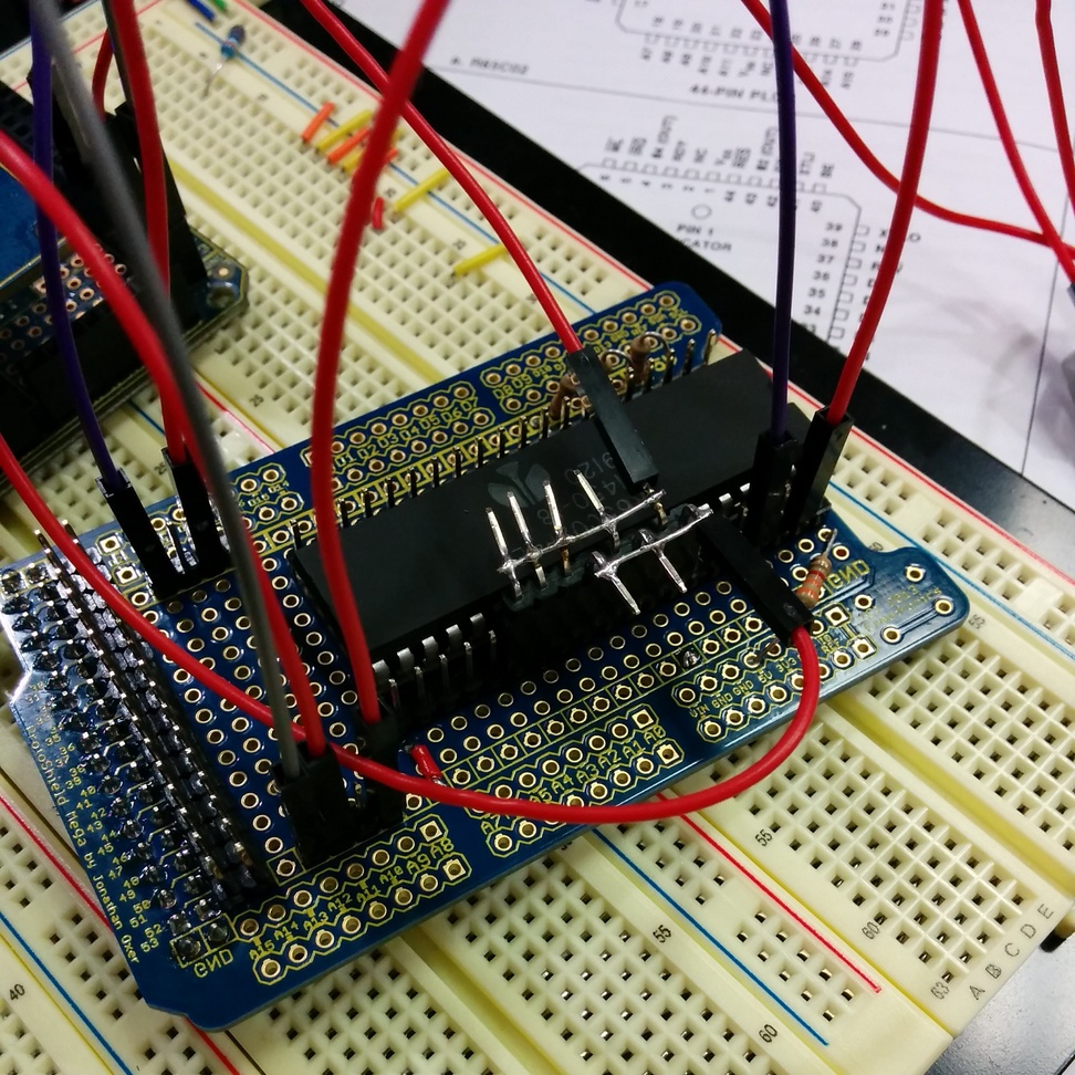
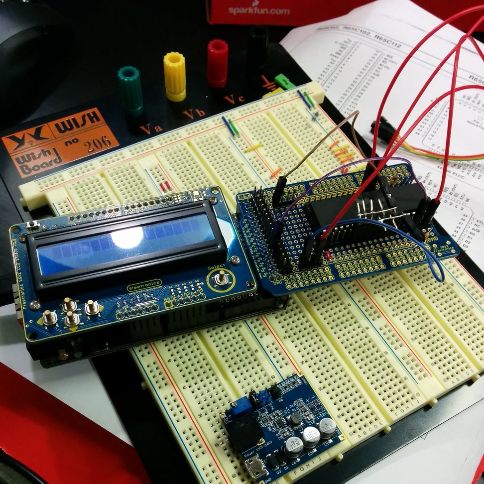
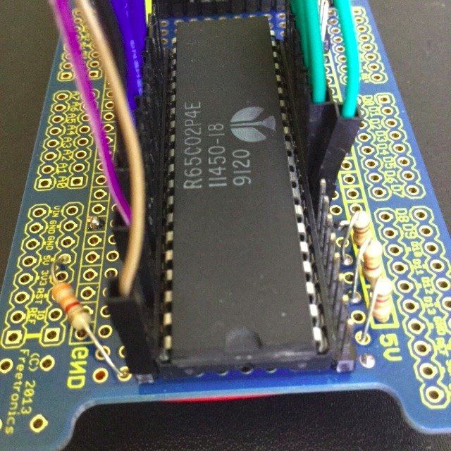
The avr11, an atmega2560 clone with a custom SPI 256kb memory.
It all started with Javascript.
In April of 2011 Julius Schmidt wrote a PDP-11 emulator that ran in a browser. I thought that this was one of the most amazing thing I had ever seen.
Late last year I ran across the link again in my Pocket backlog and spent a little time poking around the code that powered the simulator.
The PDP-11 architecture is very interesting. All the the major system components work asynchronously, co-ordinating access via the shared UNIBUS backplane. Julius’ simulator used this property and callbacks on timers to simulate components like the disk and console operating asynchronously.
I’ve written previously about the suitability of Go for writing emulators and so I thought it would be a fun project to port Julius’ work to Go. This port is going well and provided the base for porting the code to C++ for this project.
Around the same time I ran across several other projects which convinced me to try an Atmel port.
The first was the winner of last years IOCCC, a 4k Intel 8086 simulator1 which showed me that the core of a CPU simulator could be small. Ignoring main memory, you need only simulate the small number of registers defined by the architecture. The PDP-11 has 8 16bit registers, a few service registers and 32 16 bit mmu registers2 to hold mappings. This would fit even in a small microcontroller like the 328p or 32u4.
The second project was a hardware implementation of a 32bit ARM CPU running linux on an Atmel 128p. Probably built as a dare, this project showed me that reliable simulators can be built on the 8bit Atmel platform and an external device could be used to represent the larger main memory expected by the CPU being simulated.
Maybe this wasn’t as crazy as it sounded.
Why the PDP-11 ?
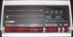
PDP-11/45 console. Image courtesy of John Holden’s PDP-11 page.
The PDP-11 is the most important minicomputer of the 1970’s.
The cost of the PDP-11 was low enough that it could be dedicated to one person or small group when mainframe computers cost so much to run that time was billed by the hour to recoup their phenomenal cost. DEC machines quickly became the platform for research and experimentation.
The PDP-11 was the machine that Ken Thompson and Dennis Ritchie developed Unix and the C programming language. As a historical artefact it has tremendous importance for anyone who is interested in computer programming or retro computing.
If you want to know why the int datatype in C defaults to 16 bits, look at the PDP-11, it was a 16 bit computer. If you want to know why a char is called a char not a byte look to way the PDP-11 stored two characters in a word.
So, what better way to learn about the PDP-11, and the history of C and Unix, than to build a simulator of the machine that started it all ?
Why build a simulator on a microcontroller?
Let’s be honest, the world doesn’t need another Arduino weather station.
Apart from wiring up LED and LCD displays I haven’t really found anything that really excites me about using microcontrollers. In some ways, the way that microcontrollers are coded and used feels very batch oriented — write some code, compile it, load it onto the micro, wait quietly to see it it worked, rinse, repeat.
I had heard a Podcast interview with one of the makers of the Pebble smart watch and learnt about the Pebble OS, a fork of FreeRTOS.
FreeRTOS looked like as a way to write interactive programs on microcontrollers, and those ideas were percolating inside my head while I was porting Julius’ Javascript simulator to Go over Christmas.
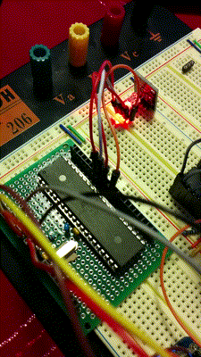
One of the nice features of Julius’ simulator was the very clean separation between the CPU logic and the memory logic. In the PDP-11 memory is just another device on the UNIBUS bus and so I began to think that if I could find some way of connecting the required 128 kilowords of memory to an Atmel the rest of the simulator should fit within the onboard SRAM.
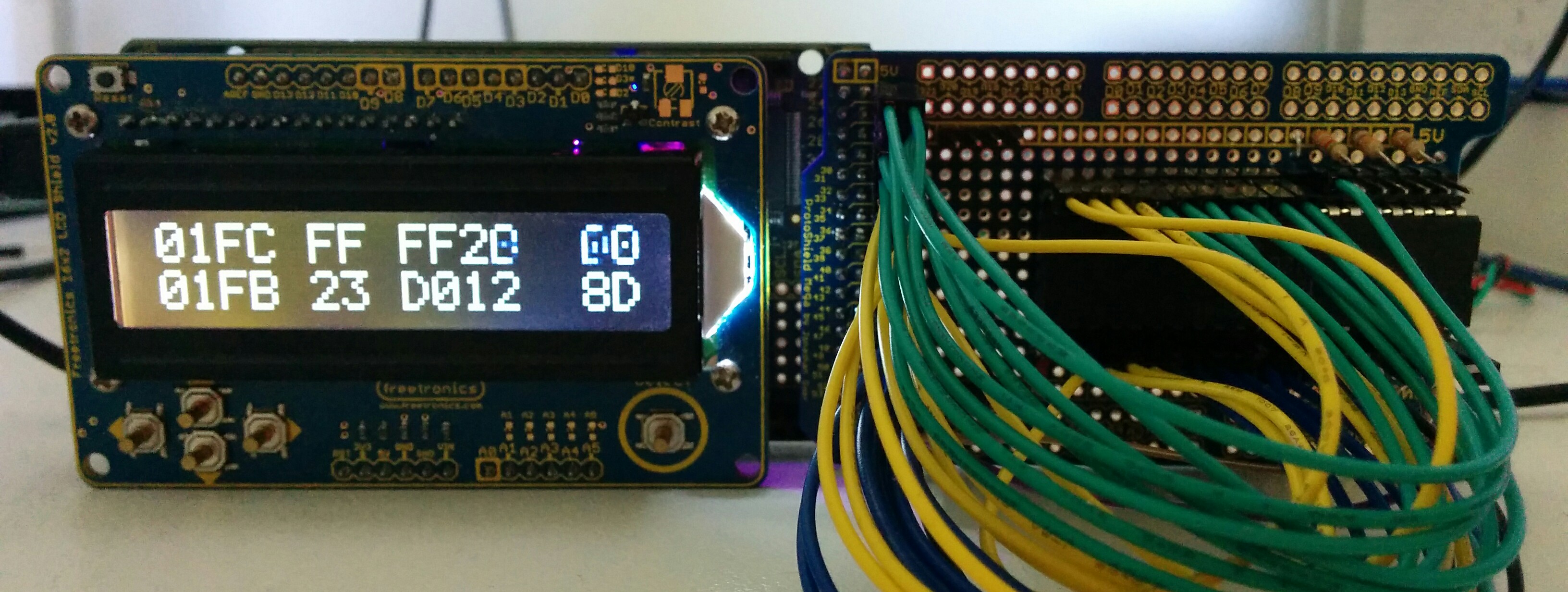
What works today
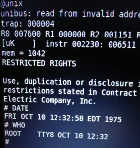
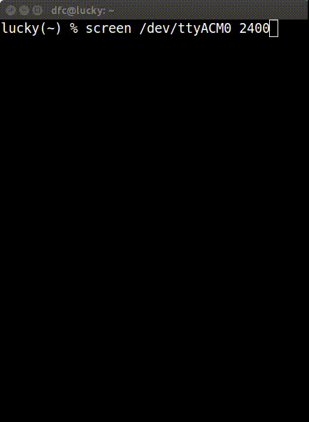
A screenshot of one of the first successful boot attempts.
Today the simulator boots V6 unix and can execute some simple commands, there are some remaining bugs in the mmu which cause the simulator to fail when larger programs (/usr/bin/cc and /usr/games/chess for example) are executed
The hardware emulated is somewhere between a PDP11/40 and PDP11/45. The EIS option (MUL and DIV) is properly emulated, but FIS (floating point is not).
Only a single RK05 drive is simulated, backed by a file on the micro SD card.
I want to improve the accuracy of the simulator so that it can run V7 unix, 2.9/2.11 BSD, RSX-11M and most importantly, the DEC diagnostics.
All these improvements are first developed on the Go port then will be integrated into the Atmel port.
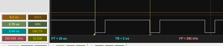
How is the performance?
Right now, not great. I don’t have a real PDP-11 for comparison, but looking at some videos on Youtube I’d have to say the simulator is at least 10x slower than an original 11/40.
I was never expecting to be amazed with the speed of this simulator, especially at this early stage. However, on a performance per watt basis, I think it’s hard to beat avr11.
The PDP-11 that this simulator models is spartan, even by the standards of the early 70s, yet still consumed over 2 kilowatts of power for the CPU and Memory (256kb). The 2.5 megabyte RK05 boot drive was another 600 watts. Real unix installations would have 3 or more drives, so there goes another 1200-1800 watts.
Compared to that, the avr11 draws well under the 500ma limit of a USB port. Although I lack equipment to measure the current draw I estimate it to be around 100ma at 5 volts which is 0.5 watts. Tell that to your data center manager.
Some specific performance issues I am aware of are:
- 32 bit register operands. Everything in the CPU is treated as a 32 bit integer during the simulation of the individual instructions. This is a hold over from the original Javascript simulation. The Atmel is internally an 8 bit CPU. There are provisions for 16 bit, double byte operations, but they come at a cost of 5x over their 8 bit counterparts. Using 32 bit operands are even more costly again.
- SPI memory. The overhead of the SPI transaction to read a word from memory is quite high. As most instructions generate at least 2 memory cycles, and can be as high as 6, fetching operands from memory consumes a lot of wall time.
Getting the code
Julius’ original Javascript implementation, from which both my Go and Atmel ports derive, is licensed under the liberal WTFPL licence. As I share similar views on software licensing, both of my projects will be similarly licensed.
The code itself is on Github. As of today it is frankly a dog’s breakfast of babies first C++ programming and Arduino hacks. As the project progresses I hope this will improve.
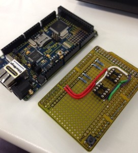
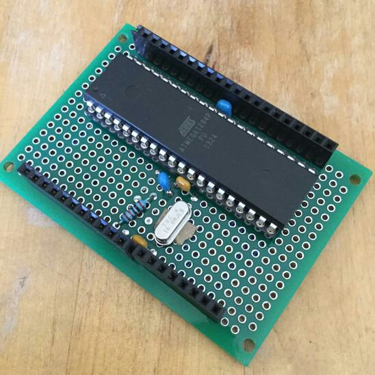
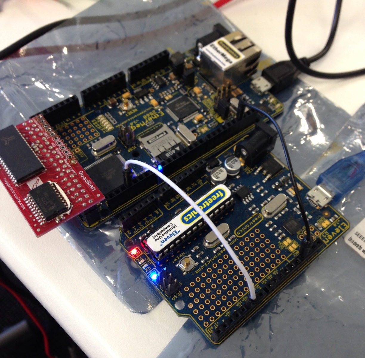
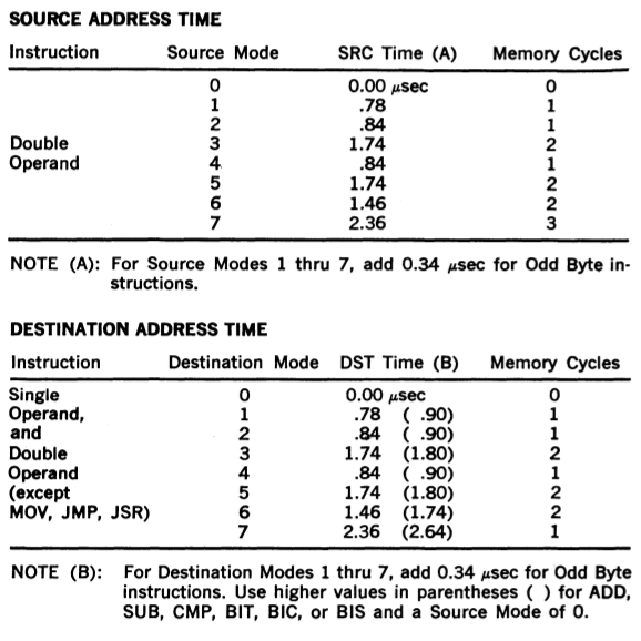
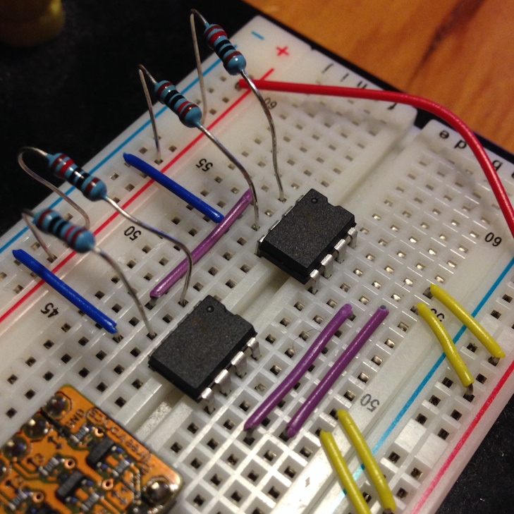
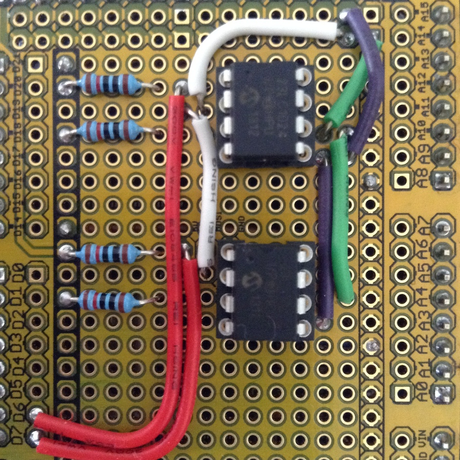
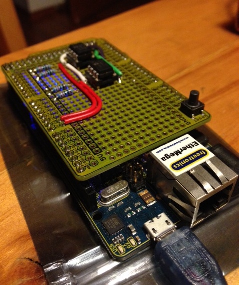
Ethermega and SPI SRAM shield (unpopulated).
However the code itself isn’t much use without the hardware. Again this is under heavy flux and I hope to improve the number platforms the simulator can run on.
The specific hardware requirements are an Atmega2560 (the older 1280 will also work, I just don’t have one to experiment with). I’m using the Freetronics Ethermega, mainly because it was what I could buy at Jaycar, but also because it has a built in micro SD card reader onboard.
The SPI SRAM shield is custom, and I’ll be writing about it in my next post.
- The author of 8086tiny has recently released a de-obfuscated version of their emulator.
- Actually Julius’ emulator cheated, there are actually 3 banks of 16 mmu registers in a real KT11 mmu, but V6 unix doesn’t use supervisor mode, so we can cheat a little here.

