Tag Archives: spi

Arduino SPI woes

A few months ago I upgraded the hardware my avr11 project ran on from the atmega2560 8bit micro to the SAM3x based Arduino Due. In doing so I lost access to the excellent QuadRAM memory expansion board, and had to find another solution for accessing the micro SD card.

For the moment, I’ve decided to go back to my SPI based SRAM shield that I built previously and this means I need to hook both the SPI SRAM shield and a Sparkfun micro SD card shield up to the Arduino Due.

Sparkfun micro SD card shield

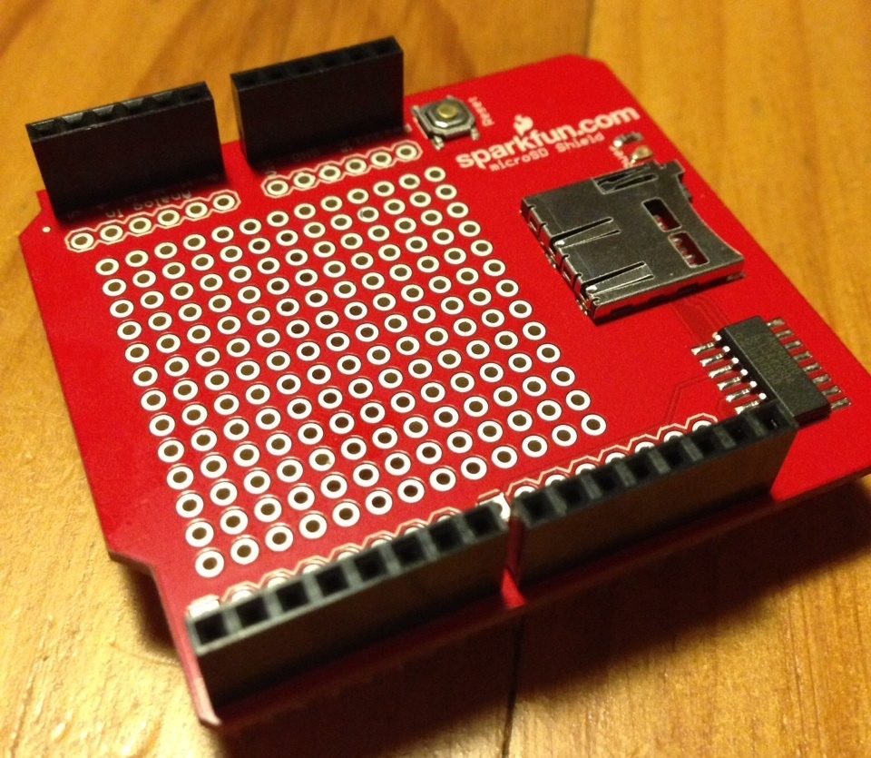
Sparkfun micro SD card shield, no ICSP header connector.

This brings me to the topic for this post; why do Arduino keep moving the SPI pins!

In the beginning there was the Arduino Uno form factor, SPI was available on both pins 11, 12 and 13 as well as the dedicated ICSP header.

Arduino Uno

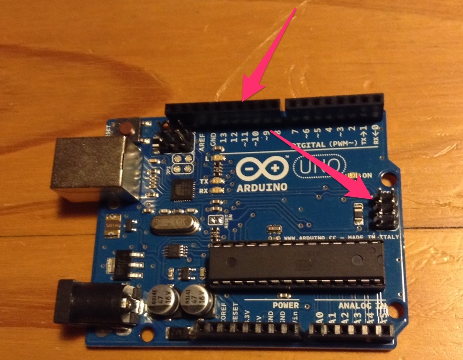
SPI is available on pins 11, 12 and 13, as well as the ICSP header.

Then the Arduino mega platform came out, with the Atmel 2560 chipset and the larger shield sizes.

Freetronics Ethermega 2560

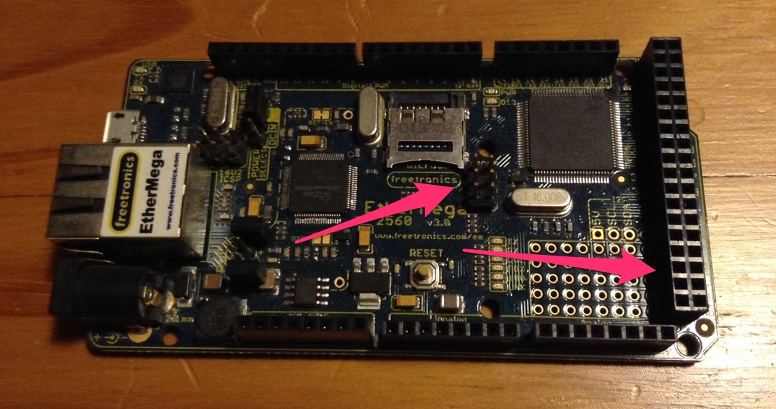
SPI has moved to pins 51, 52 and 53, as well as the ICSP header.

SPI is no longer available on pins 11, 12 and 13, but has moved to pins 51, 52 and 32. It remains available on the ICSP header, which is the area that Arduino is pushing shield makers to use. Unfortunately shield makers are steadfastly ignoring the recommendations from Arduino and none of the SD card shields I ca find have a connector to route the ICSP header upwards as you add additional shields. The blanks shields from Freetronics don’t even make it an option.

This brings me to the Arduino Due, which I needed to get the grunt to run my avr11 simulator.

Due

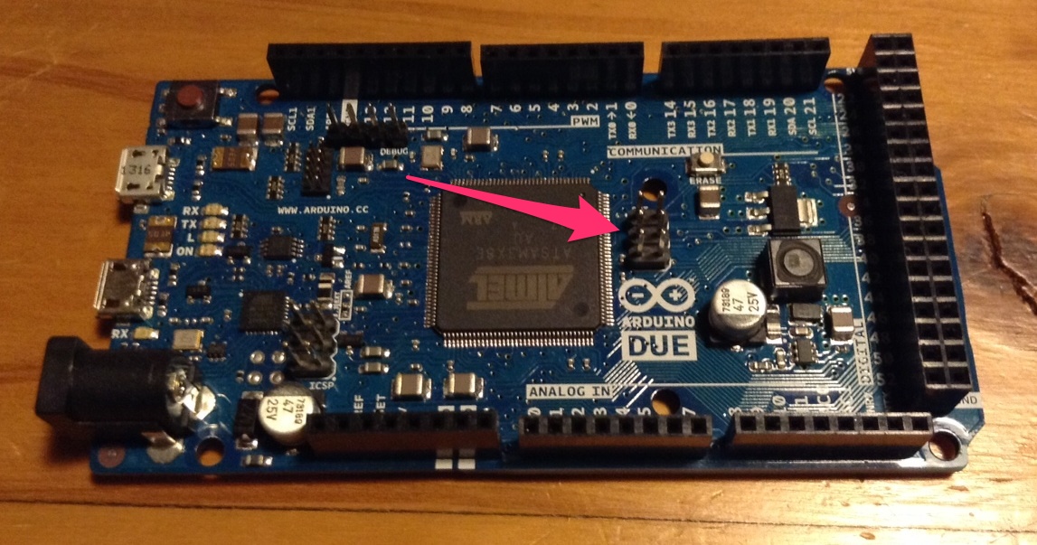
SPI available on the ICSP header, only.

To use SPI on the Due I need to somehow route the ISCP connector to pins 11, 12 and 13.

Nasty

Nasty.

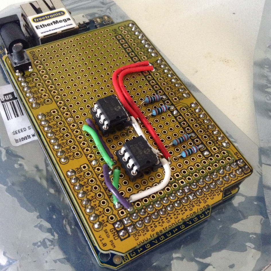
The best solution I had at the time was to raise the shield away from the Due using stacked headers, then route the ISCP signals to the pins that the board (and the SDFat software) expected to find them with some jumper cables. Out of shot, pins 11, 12 and 13 were bent upwards so they did not make contact with the sockets on the Due board.

This was where the project stalled for a few months.

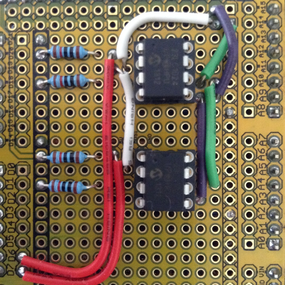
Recently I’ve had some time to come back to this project, and the first order of business was solving the SPI problem. It was clear that pins 11, 12 and 13 were the rightful place for the SPI signals and to try to route them anywhere else would be fruitless. So, with an official Arduino expansion shield in hand, I made myself an SPI adapter board.

ICSP adapter

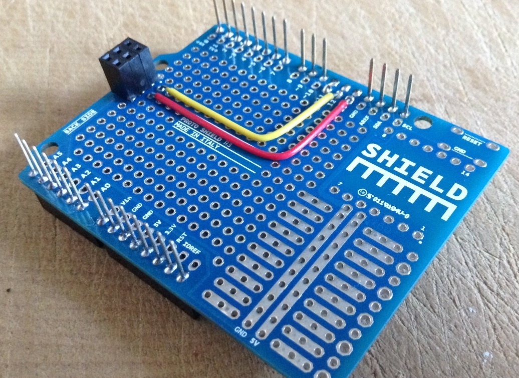
Pins 11, 12 and 13 are removed, but still connect to the stacked header on the opposite side of the board.

The board is very simple, all the usual Arduino Uno pins are passed through as expected, however pins 11, 12 and 13 are routed to the ICSP header to match the Arduino documentation.

icsp top view

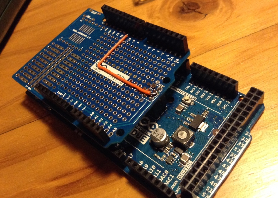
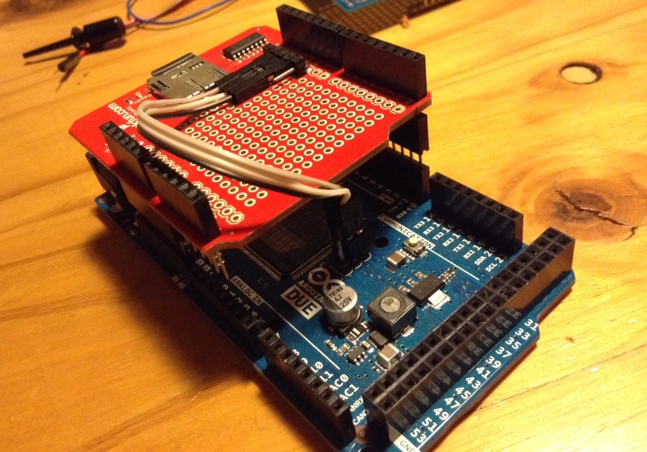
Adapter board mounted on an Arduino Due.

Here is a picture of the shield mounted on the Due. The trace for pin 11 is run on this side of the board to avoid crossing pin 13. I felt this was important as SPI can run upwards of 16 Mhz, however I’m not sure how much improvement this will make as these traces are still long and unshielded.

final

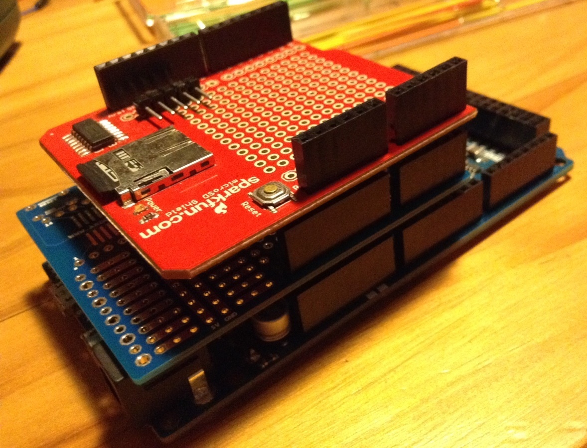
The final result, more compact and much more stable.

Here is a shot of result. The SD shield is mounted without floating pins or jumper wires and additional shields can be mounted on top of the SD card shield with the original locations of the SPI pins respected.

avr11: building an SPI SRAM shield for an Arduino Mega

spi-sram-shield

SPI SRAM shield mounted on an Freetronics Ethermega

In my previous post I had figured out that I could capture memory accesses in my simulator and send them elsewhere.

In version 1 of the design I (ab)used the onboard mini SD card to simulate the entire address space. This was a very 1950’s solution and came with matching performance.

Still, it did give me confidence that this project was possible and so I located a kit which would give me a better performing memory subsystem. I duly ordered the kit from Colin Irwin but didn’t know how long it would take to get here from France.

Trolling around eBay I had found various EEPROM solutions like this one which I thought I could adapt. The board wasn’t directly usable as it was configured for 2 wire I2C, not 3 wire SPI, but it suggested to me that I could build a shield to hold some SRAM chips to get my project going while I waited for the XRam shield to arrive.

There is a common SRAM chip, the Microchip 23K256, which is a 32 kilobyte chip with an SPI interface. I’ve seen it used in various PIC designs, and is an option on the Propeller PMC.

The 23K256 isn’t as common in Arduino designs because of one major flaw; it’s a 3v3 part. This would mean adding a level converter to the shield and being careful not to drop 5 volts across any of the pins on the chip.

There was also the problem of capacity. To get to 256 kilobytes I would need 8 chips on the same SPI bus, and a logic level converter, not counting the onboard SPI devices like the micro SD card and the Wiznet ethernet chip that come with the Ethermega. This was likely to get more complicated than I was planning on, so I continued to look for an alternative SRAM part.

Version 2, the 23LC1024

Luckily I didn’t have to look very far. The Microchip 23LC1024 has 4 times the capacity, and can operate at 5 volts. This meant I would only need two chips to get 256kb and would only need to dedicate two pins to driving the Chip Select lines on the SRAM ICs.

As I live in Australia, there is a difference between choosing the part you want, and actually being able to buy it. While most of the Microchip stock appeared to be in the UK, I found the last two chips in stock at a Element 14, and ordered them straight away. Spares? Pfft, those are for people with no self confidence.

breadboardin

wow. such unstable. so noise. very breadboard

Spelunking on the Arduino forums had yielded some war stories and a nice SpiSRAM library to interface with the chips. It also came with a small ram test sketch.

My first attempts to integrate the 23LC1024s on the breadboard wasn’t very successful. Even though I follow the application note I wasn’t able to get the chips to reliably pass the SRAM test. Sometimes the data would be written perfectly, other times it would just be garbage.

By default the 16Mhz Atmel parts drive the SPI pins at 4Mhz. From reading other blogs it was clear that this sort of frequency is outside what the breadboard is designed for, not to mention the large patch leads between the Ethermega and the breadboard.

Increasing the SPI divider to slow down the transactions sort of worked, but it was clear I wouldn’t be able to hook the SRAM up to the avr11 in this condition so I’d need to build a proper shield to hold the ICs.

closeup

Closeup of the shield. No, you may not see the under-side.

A few days and another trip to Jaycar later, I had all the parts I needed. A few hours bodging at the local hacker space and I had reproduced my design onto a prototyping shield allocating pins D6 and D7 as the chip select pins.

I took the shield home, plugged in the chips and both banks worked first time! Getting cocky I loaded the avr11 sketch and discovered that the micro SD card had failed to initialise, WTF! Reloading the sketch, the SD card worked fine, but the SRAM test showed garbage.

The source of the problem turned out to be the default state of the digital pins on the Arduino. The way SPI works is all the components on the SPI bus share three lines, MISO (master in, slave out), MOSI (master out, slave in), and SCLK (a clock line driven by the master). Additionally every device has its own Chip Select line which must be held high to inhibit the device unless you want to talk to it.

To talk to an individual device, you lower the CS line connected to that chip and read and write data on MOSI/MISO, toggling the SCLK line. All the other devices which have their CS lines high are supposed to hold their MISO and MOSI at a high impedance and ignore transactions on the bus.

The problem is, when the Arduino resets, all the digital lines are set to input and are low; you don’t want an Arduino with no sketch loaded suddenly sending 5volts out of every digital pin. In effect all the Chip Select lines could be active, meaning all the components are listening to the transaction and trying to interact with the master.

The solution I came up with was to ensure that all the digital pins are set to output and held high before calling any of the SD.begin() or SPI.begin() functions.

void setup(void) {
  // setup all the SPI pins, ensure all the devices are deselected
  pinMode(4, OUTPUT); digitalWrite(4, HIGH);    // micro sd
  pinMode(6, OUTPUT); digitalWrite(6, HIGH);    // bank0
  pinMode(7, OUTPUT); digitalWrite(7, HIGH);    // bank1
  pinMode(10, OUTPUT); digitalWrite(10, HIGH);  // wiznet
  pinMode(53, OUTPUT); digitalWrite(53, HIGH);  // atmega2560 SS line
  ... more setup code

In effect this disables all the SPI devices until their various begin() functions were called to configure them.

Maybe this wasn’t the best solution, but since I implemented it the SRAM and SD card have been perfectly stable so I consider it case closed.

Coming up

This post takes me up to the present day. Right now I have a XRam kit to be built up, and a QuadRAM which was sold to me by a very kind blogger who wasn’t using it, sitting on my desk.

Both the XRam and QuadRAM are functionally identical and each can provide more that the 256kb of SRAM needed for this project which is effectively directly integrated into the atmega2560’s address space.

avr11: how to add 256 kilobytes of ram to an Arduino

18 bits of core memory

In Schmidt’s original javascript simulator, and my port to Go, the 128 kilowords (256 kilobytes) of memory connected to the PDP-11 is modeled using an array. This is a very common technique as most simulators execute on machines that have many more resources than the machines they impersonate.

However, when I started to port my Go based simulator to the Arduino, the problem I faced was the Atmel does not support an address space larger than 64 kilobytes, and more immediate, all the 8 bit Atmega models ship with somewhere between 2kb and 8kb of addressable memory.

Version 0, use the Arduino itself

Deciding to put that problem to the side until I saw if the job of rewriting (and dusting off my long obsolete C coding skills) was achievable, the first version of the simulator I wrote did use a simple array for UNIBUS memory.

#define MEMSIZE 2048
uint16_t memory[MEMSIZE];

Using an Atmega2560 I was able to create a memory of 4096 bytes, which was enough to bring up the simulator and run the short 29 word bootstrap program which loaded the V6 Unix bootloader into memory.

Sadly the bootloader would fault the simulated CPU almost immediately as the first thing the bootloader does is zero the entire address space, quickly running past the end of the array and overwriting something important.1

However, this did let me get to the point that the CPU and RK11 drive simulators were working well, not to mention figuring out how to write a large multi file program using the Arduino IDE environment.

Memory lives somewhere else

A revelation I have recently arrived at is that, from the point of view of a CPU, memory is not part of the processor. Data in a real CPU moves into and out of the device in a very orchestrated manner and in avr11 this is no different.

Any instruction that references memory, either directly loading data into a register via the MOV instruction, or indirectly using one of the PDP-11’s addressing modes always boiled down to a read or write function which linked the CPU to the simulated UNIBUS.

For example, in the Go version of the simulator, memory []uint16 belongs to the unibus struct. In the C++ version for Atmel this is enforced further by there being no extern uint16_t memory[MEMSIZE]; definition exposed in unibus.h.

In short, there is no way for the CPU to observe memory, it has to ask the UNIBUS to read or write data on its behalf, and this gave me the opportunity to solve the problem of limited memory space available on the Atmel devices I had access to.

Version 1, I am a bad person

At this point I’m sort of telling the story backwards. I had found a product which would give me far more memory than I needed for this project, but it took several weeks to arrive and comes as a kit, which will involve some tricky SMD soldering.

In the interim I found myself during the Christmas to New Years break with a simulator that I felt was working well enough to try something more adventurous if I could only find some way to emulate the backing array for the core memory. I didn’t really care about speed, I just wanted to see if the simulator could handle the more complicated instructions of the Unix kernel.

“Why not use the SD card?” I said to myself. I was after all already loading some of the blocks off the RK05 disk pack image from the card, so why not just make another image file and make that back the core memory. The mini SD card probably wouldn’t last very long, but I have a pile of cheap cards so why not try it.

 void pdp11::unibus::write8(uint32_t a, uint16_t v) {
    if (a < 0760000) {
       if (a & 1) {
         core.seek(a);
         core.write(v & 0xff);
         //memory[a >> 1] &= 0xFF;
         //memory[a >> 1] |= v & 0xFF << 8;

All it took was setting up a new SD::File, called core and rewriting the access to the memory array with seeks and writes to the backing file (obviously doing the same for the read paths).

Amazingly it worked, on the second or third attempt, and although it was very slow I was able to use this technique to boot the simulator a very long way into the Unix boot process. I posted a video of the bootup to instagram.

Even more amazingly I didn’t wear out the mini SD card, and still haven’t. This is probably mostly due to the wear leveling built into the card2 but I also stumbled into a fortuitous property of the SD card itself, and the Arduino drivers on top.

All SD cards, well certainly SD and mini SD cards, mandate that you read and write to them in units of pages. Pages happen to be 512 bytes, a unit which clearly descends from the days of CF cards which emulated IDE drives.

This means the Arduino SD class maintains a buffer of 512 bytes, (which comes out of your precious SRAM allotment) that in effect operated as a cache for my horrible all swap based memory system. For example, when the bootloader program zeros all the memory in the machine, rather than writing to the SD card 253,952 times3, the number of writes was probably much smaller, say 500 writes.

Obviously as it was not designed for this purpose the cache would fail badly during a later part of the bootup where the kernel code is copied (about 90 kilowords of it) from one memory area to another. Each read or write would land on a different SD card page, causing it to flush the old buffer, read in the new buffer, then reverse the process.

But it worked, and gave me confidence to investigate some more ambitious designs for a memory solution.

In my next blog post I’ll talk about version 2 of my memory system, the one that I finally got me booting to the # prompt.


  1. I considered using a SAM3X atmel32 style board, like the Arduino Due as they have both a more powerful CPU and close to 96 kilobytes of addressable memory, but that is only 48 kilowords, less than half of what I need to simulate the full 128 kiloword address space of the PDP-11.
  2. The internet is divided on the question of “Do cheap mini SD cards have wear leveling?”. Part of the problem is the definition of cheap changes rapidly over time, making advice written 12 months ago inaccurate. My view is that cards of any capacity you can buy today require so much error correction logic that you get the wear leveling logic for free.
  3. On the PDP the top 4 kilo words of memory (8kb) is reserved for the IO devices, so while the UNIBUS talks in 18 bit addresses, the top 4096 words is not mapped to memory, and doesn’t need to be cleared. In fact clearing the IO page memory would be catastrophic.